3.9.2. TX DL Shim Wrapper
By default, the samples sent out on the user interface will be the parameterized pattern (DLW, DLCW), DLCW will be inserted into the real-time samples at the rising edge detection of the SYSREF. The switchover from pattern data to real-time sample data happens after rx_in_sync is asserted, and it is aligned with the SYSREF rising edge event. The RX signal, rx_in_sync is required to ensure that the sample data MUX at the TX side is switched only after RX is in SYNC and receiving the data from TX. This is to establish the RX reception before switching to Sample Data. This is not a timing-critical signal and can be routed to TX with relaxed timing. This rx_in_sync can be connected from RX FPGA to TX FPGA on board or logically by software reading the RX status output and driving the TX control input. Users can refer to the output status signal, tx_user_data_sel to confirm when the IP is ready to receive user data.
To ensure deterministic latency operation across the link, the F-Tile Serial Lite IV Intel® FPGA IP TX logic is modified in such a way to make sure the ALIGN counter is enabled based on the first rising edge detection of SYSREF, so that the ALIGN CW insertion is aligned to the SYSREF event. The ALIGN_PERIOD will follow the SYSREF_PERIOD set in the SYSREF Pulse Generator.
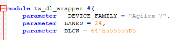
The TX DL shim wrapper module consists of a TX Proc logic (datapath MUX + DLCW/DLW generator) and a DCFIFO. The DLCW/DLW generator provides a user-programmable parameter to set for the DLCW pattern with DLW recommended to be the complement of the DLCW. The DLCW is inserted for 1 user clock cycle at the rising edge of the SYSREF pulse followed by DLW. The DLCW pattern is preset to 555555D5 per lane in the design module.
| Signal Name | Direction | Type | Description |
|---|---|---|---|
| tx_user_clk | Input | Wire | Input clock from user clock source. |
| tx_core_clkout | Input | Wire | Input clock from F-Tile Serial Lite IV Intel® FPGA IP tx_core_clk. |
| tx_rst | Output | Reg | Active high asynchronous reset. Asserts the reset when IP core tx_core_rst is asserted. |
| sysref | Input | Wire | Periodic pulse signal from SYSREF Generator. |
| rxinsync | Input | Wire | Input signal from the RX DL wrapper to indicate DLCW word has been received on all the lanes and the data has been passed to the RX Proc logic. |
| tx_link_up | Input | Wire | TX link up signal from F-Tile Serial Lite IV Intel® FPGA IP core. |
| tx_data | Input | Wire [(N*2*64)-1:0] | Avalon® streaming interface Data signal from the user traffic generator. |
| tx_valid | Input | Wire | Avalon® streaming interface Valid signal from the user traffic generator. |
| tx_ready | Input | Wire | Avalon® streaming interface Ready signal from F-Tile Serial Lite IV Intel® FPGA IP core. |
| tx_user_data_sel | Output | Wire | Output signal connected to the user traffic generator to indicate that it is ready to receive user data. |
| tx_data_out | Output | Wire [(N*2*64)-1:0] | Output Avalon® streaming interface Data to F-Tile Serial Lite IV Intel® FPGA IP core. |
| tx_data_valid | Output | Wire [(N*2)-1:0] | Output Avalon® streaming interface Valid to F-Tile Serial Lite IV Intel® FPGA IP core. |
| fifo_pfull | Output | Wire [(N*2)-1:0] | Output status signal to indicate the internal FIFO is under partial full status. |
| fifo_full | Output | Wire [(N*2)-1:0] | Output status signal to indicate the internal FIFO is under full status. |