3.9.3. RX DL Shim Wrapper
After the F-Tile Serial Lite IV Intel® FPGA IP is aligned/RX link is up, data will be ready to be passed to user logic or the RX DCFIFO/buffer as shown in the figure.. The data will be written to the RX DCFIFO/buffer. The RX buffer triggers the RBD delay on every detected SYSREF rising edge and at the end of the RBD_Delay, checks whether the DLCW word has been received on all the RX lanes and then only pass the data to the RX Proc logic and asserts the rx_in_sync signal. The RBD delay should manage the SL4 IP skew variation between lanes as well as any variation due to the transfer of real-time samples over different clock domains.
Since the FEC alignment marker insertion cycles (4 cycles), cadence cycles (1 cycle), and other scenarios (paired CWs, 2 cycles) can occur consecutively or concurrently, the worst case number of tx_ready de-assertion cycles is seven. Also, if taking into consideration the maximum of five parallel rx_core_clk cycles of the inter-lane skews scenario, the RBD value must be programmed to ensure that data is read from RX buffer when the buffer occupancy is ≥13, this is to ensure the continuity of data when the F-Tile Serial Lite IV Intel® FPGA IP TX would insert holes due to its protocol overhead in the worst case scenario mentioned previously.
The RBD value must be greater than the latency of TX+RX (including TX DL shim and RX DL shim) in the user_clk cycle, plus an additional ≥13 to prefill the RX DCFIFO.
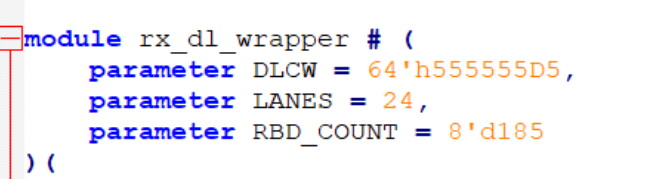
For example, the latency of TX+RX = 172 user clock cycles, prefill value =13. So, the total delay value to be set is 185. The total latency of TX+RX (including TX DL shim and RX DL shim) will be a deterministic value of 185 user clock cycles. Users can set the RBD_COUNT parameter value to 8’d185.
| Signal Name | Direction | Type | Description |
|---|---|---|---|
| rx_user_clk | Input | Wire | Input clock from user clock source. |
| rx_core_clkout | Input | Wire | Input clock from F-Tile Serial Lite IV Intel® FPGA IP rx_core_clk. |
| rx_rst | Output | Wire | Active high asynchronous reset. Asserts the reset when IP core rx_core_rst is asserted. |
| sysref | Input | Wire | Periodic pulse signal from SYSREF Generator. |
| rxinsync | Output | Reg | Indicates DLCW word has been received on all the lanes and the data has been passed to the RX Proc logic. |
| rx_data | Input | Wire [(N*2*64)-1:0] | Avalon® streaming interface Data signal from F-Tile Serial Lite IV Intel® FPGA IP core. |
| rx_valid | Input | Wire | Avalon® streaming interface Valid signal from F-Tile Serial Lite IV Intel® FPGA IP core. |
| rx_fifo_ready_empty | Output | Wire | Output status signal to indicate the internal FIFO hits empty status. |
| rx_fifo_rd_pfull_out | Output | Wire [5:0] | Output status signal to indicate the internal FIFO hits partial full status. |
| rx_data_out | Output | Wire [(N*2*64)-1:0] | Avalon® streaming interface Data to user traffic checker. |
| rx_data_valid | Output | Wire | Output Avalon® streaming interface Valid to user traffic checker. |