AN 775: Generating Initial I/O Timing Data and I/O Element Delays for Altera FPGAs
ID
683103
Date
9/29/2025
Public
2.1. Step 1: Create Simple Flip-Flop Design
2.2. Step 2: Define I/O Delay Chain and Clock Settings
2.3. Step 3: Specify Device Operating Conditions
2.4. Step 4: View IOE Timing Delay with Report Path
2.5. Scripted IOE Information Generation
2.6. Document Revision History for AN 775: Generating Initial I/O Timing Data and I/O Element Delays for Altera FPGAs
1.1. Step 1: Synthesize a Flip-flop for the Target Altera FPGA Device
Follow these steps to define and synthesize the minimum flip-flop logic to generate initial I/O timing data:
- Create a new project in Quartus® Prime Pro Edition software version 25.3.
- Click Assignments > Device, specify your target device Family and a Target device. For example, select the AGFA014R24 Agilex™ FPGA portfolio FPGA.
- Click File > New click Verilog HDL File.
- Create a simple flip-flop design, as the following shows:
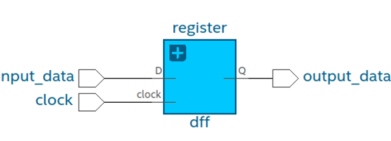
module dff ( input D, input clock, output reg Q); always @ (posedge clock) begin Q <= D; end endmodule - Repeat step 3 to create the flip-flop design that connects two instances of the DFF, as the following shows:
module gclk(
     input clock,
     input input_data,
     output output_data);
     dff register (.clock(clock),.D(input_data), .Q(output_data));
endmodule
Figure 2. DFF with Pin Connections
- To synthesize the DFF, click Processing > Start > Start Analysis & Synthesis. Synthesis generates the minimum design netlist required to obtain I/O timing data.