AN 775: Generating Initial I/O Timing Data and I/O Element Delays for Altera FPGAs
ID
683103
Date
9/29/2025
Public
2.1. Step 1: Create Simple Flip-Flop Design
2.2. Step 2: Define I/O Delay Chain and Clock Settings
2.3. Step 3: Specify Device Operating Conditions
2.4. Step 4: View IOE Timing Delay with Report Path
2.5. Scripted IOE Information Generation
2.6. Document Revision History for AN 775: Generating Initial I/O Timing Data and I/O Element Delays for Altera FPGAs
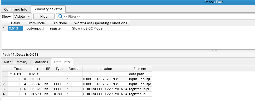
2.4.1. Example 1: Viewing the Input Element Delay in Reports
In the following example, Report Path shows the maximum delay of input pin to register for the Slow mode at 0C Model operating condition.
Figure 15. Input Element Delay (Input Delay Chain Setting = 0)