Intel® Arria® 10 and Intel® Cyclone® 10 GX Avalon Streaming Hard IP for PCIe* Design Example User Guide
1.5. Compiling and Testing the Design in Hardware
Figure 8. Procedure
Figure 9. Software Application to Test the PCI Express Design Example on the Intel® Arria® 10 GX FPGA Development KitA software application running on a Windows PC performs the same hardware test for all of the PCI Express Design Examples.
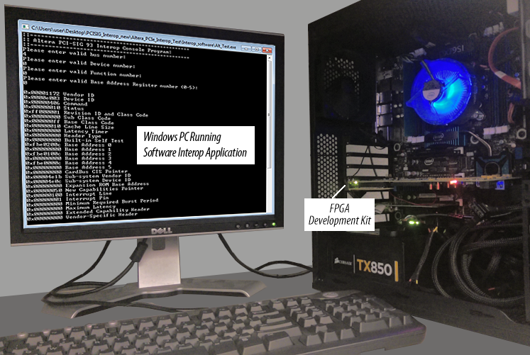
The software application to test the PCI Express Design Example on the Intel® Arria® 10 GX FPGA Development Kit is available on both 32- and 64-bit Windows 7 platforms. This program performs the following tasks:
- Prints the Configuration Space, lane rate, and lane width.
- Writes 0x00000000 to the specified BAR at offset 0x00000000 to initialize the memory and read it back.
- Writes 0xABCD1234 at offset 0x00000000 of the specified BAR. Reads it back and compares.
If successful, the test program displays the message 'PASSED'
Follow these steps to compile the design example in the Quartus Prime software:
- Launch the Quartus Prime software and open the pcie_example_design.qpf file for the example design created above.
- On the Processing > menu, select Start Compilation.
The timing constraints for the design example and the design components are automatically loaded during compilation.
Follow these steps to test the design example in hardware:
- In the <example_design>/software/windows/interop directory, unzip Altera_PCIe_Interop_Test.zip.
Note: You can also refer to readme_Altera_PCIe_interop_Test.txt file in this same directory for instructions on running the hardware test.
- Install the Intel® FPGA Windows Demo Driver for PCIe on the Windows host machine, using altera_pcie_win_driver.inf.
Note: If you modified the default Vendor ID (0x1172) or Device ID (0x0000) specified in the component parameter editor GUI, you must also modify them in altera_pcie_win_driver.inf.
- In the <example_design> directory, launch the Quartus Prime software and compile the design (Processing > Start Compilation).
- Connect the development board to the host computer.
- Configure the FPGA on the development board using the generated .sof file (Tools > Programmer).
- Open the Windows Device Manager and scan for hardware changes.
- Select the Intel® FPGA listed as an unknown PCI device and point to the appropriate 32- or 64-bit driver (altera_pice_win_driver.inf) in the Windows_driver directory.
- After the driver loads successfully, a new device named Altera PCI API Device appears in the Windows Device Manager.
- Determine the bus, device, and function number for the Altera PCI API Device listed in the Windows Device Manager.
- Expand the tab, Altera PCI API Driver under the devices.
- Right click on Altera PCI API Device and select Properties.
- Note the bus, device, and function number for the device. The following figure shows one example.
Figure 10. Determining the Bus, Device, and Function Number for New PCIe Device
- In the <example_design>/software/windows/interop/Altera_PCIe_Interop_Test/Interop_software directory, click Alt_Test.exe.
- When prompted, type the bus, device, and function numbers and select the BAR number (0-5) you specified when parameterizing the IP core.
Note: The bus, device, and function numbers for your hardware setup may be different.
- The test displays the message, PASSED, if the test is successful.
Note: For more details on additional design implementation steps such as making pin assignments and adding timing constraints, refer to the Design Implementation chapter.