2.4.1. Example: DQ Pin Swizzling Within DQS group for x32 DDR4 interface
Example: DQ Pin Swizzling Within DQS group for x32 DDR4 interface
This example uses the lane placement of the following table, using a memory device of x8 width.
| Lane Number | BL0 | BL1 | BL2 | BL3 | BL4 | BL5 | BL6 | BL7 |
|---|---|---|---|---|---|---|---|---|
| Default placement | DQ[0] | AC0 | AC1 | AC2 | DQ[1] | DQ[2] | DQ[3] | GPIO |
| Lane | Pin Index | DDR4 x32 (Default Placement) | After Swizzling / Swapping |
|---|---|---|---|
| BL0 | 11 | MEM_DQ[7] | MEM_DQ[6] |
| 10 | MEM_DQ[6] | MEM_DQ[5] | |
| 9 | MEM_DQ[5] | MEM_DQ[7] | |
| 8 | MEM_DQ[4] | MEM_DQ[4] | |
| 7 | |||
| 6 | MEM_DM_N[0] | MEM_DM_N[0] | |
| 5 | MEM_DQS_C[0] | MEM_DQS_C[0] | |
| 4 | MEM_DQS_T[0] | MEM_DQS_T[0] | |
| 3 | MEM_DQ[3] | MEM_DQ[0] | |
| 2 | MEM_DQ[2] | MEM_DQ[2] | |
| 1 | MEM_DQ[1] | MEM_DQ[1] | |
| 0 | MEM_DQ[0] | MEM_DQ[3] |
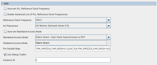
To achieve this swizzling in DQS group 0, you must enter PIN_SWIZZLE_CH0_DQS0=3,1,2,0,4,7,5,6; in the Pin Swizzle Map field in the PHY section of the High-level Configuration tab in the EMIF IP parameter editor.
Figure 17. Entering a PIN_SWIZZLE Specification
| Lane | Pin Index | DDR4 x32 (from table) | After Swizzling / Swapping |
|---|---|---|---|
| BL5 | 71 | MEM_DQ[23] | MEM_DQ[17] |
| 70 | MEM_DQ[22] | MEM_DQ[22] | |
| 69 | MEM_DQ[21] | MEM_DQ[21] | |
| 68 | MEM_DQ[20] | MEM_DQ[20] | |
| 67 | |||
| 66 | MEM_DM_N[2] | MEM_DM_N[2] | |
| 65 | MEM_DQS_C[2] | MEM_DQS_C[2] | |
| 64 | MEM_DQS_T[2] | MEM_DQS_T[2] | |
| 63 | MEM_DQ[19] | MEM_DQ[19] | |
| 62 | MEM_DQ[18] | MEM_DQ[18] | |
| 61 | MEM_DQ[17] | MEM_DQ[23] | |
| 60 | MEM_DQ[16] | MEM_DQ[16] |
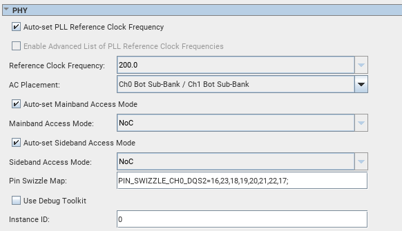
To achieve this swizzling in DQS Group 2, you must enter PIN_SWIZZLE_CH0_DQS2=16,23,18,19,20,21,22,17; in the Pin Swizzle Map field of the PHY section of the High-level Configuration tab in the parameter editor.
Figure 18. Entering a PIN_SWIZZLE Specification
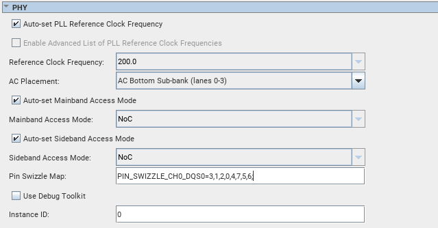
You can enter multiple specifications in the Pin Swizzle Map field, each separated by a comma.
Figure 19. Entering Multiple PIN_SWIZZLE Specifications