External Memory Interfaces Agilex™ 7 M-Series FPGA IP Design Example User Guide
ID
772632
Date
7/07/2025
Public
A newer version of this document is available. Customers should click here to go to the newest version.
1. About the External Memory Interfaces Agilex™ 7 M-Series FPGA IP
2. Design Example Quick Start Guide for External Memory Interfaces Agilex™ 7 M-Series FPGA IP
3. Design Example Description for External Memory Interfaces Agilex™ 7 M-Series FPGA IP
4. Document Revision History for External Memory Interfaces Agilex™ 7 M-Series FPGA IP Design Example User Guide
2.1. Creating an EMIF Project
2.2. Generating and Configuring the EMIF IP
2.3. Parameterizing the External Memory Interface for HPS IP
2.4. Configuring DQ Pin Swizzling
2.5. Generating the Synthesizable EMIF Design Example
2.6. Back Annotating Pin Placement and I/O Standard Assignments
2.7. Generating the EMIF Design Example for Simulation
2.8. Pin Placement for Agilex™ 7 M-Series EMIF IP
2.9. Compiling the Agilex™ 7 M-Series EMIF Design Example
2.10. Using the EMIF Design Example with the Test Engine IP
2.11. Generating the EMIF Design Example with the Performance Monitor
2.4.1. Example: DQ Pin Swizzling Within DQS group for x32 DDR4 interface
2.4.2. Example: Byte Swizzling for a x32 DDR4 interface, using a memory device of x8 width
2.4.3. Combining Pin and Byte Swizzling
2.4.4. Example: Swizzling for a x32 + ECC interface
2.4.5. Example: Swizzling for a 2Ch x32 + ECC interface
2.4.6. Example: Byte Swizzling for Lockstep Configuration
2.6. Back Annotating Pin Placement and I/O Standard Assignments
To compile a design that instantiates an Agilex™ 7 M-Series EMIF IP, you must explicitly define a legal placement and I/O standard for for all EMIF pins.
The Quartus® Prime Pro Edition software can infer most of the required pin locations and I/O standard assignments if you have properly constrained the following pins:
- Differential P-side reference clock input
- RZQ site
- MEM_RESET_N
To define pin placement and I/O standards and generate a programming .sof file, follow these steps:
- Open the project's .qsf file, and at the end of the file, define a correct placement for RZQ, MEM_RESET_N and the PSide of the reference clock, for example:
set_location_assignment PIN_T63  -to ref_clk_clk
set_location_assignment PIN_AC58 -to emif_io96b_0_oct_0_oct_rzqin
set_location_assignment PIN_AB59 -to emif_io96b_0_mem_reset_n_0_mem_reset_n
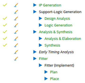
- Compile your project up to the placement stage of the Fitter.
Figure 25. Compilation up to the Placement Stage of the Fitter
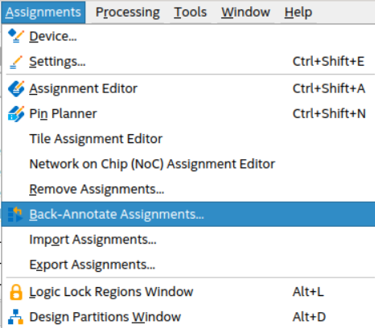
- Click Assignments > Back-Annotate Assignments
Figure 26. Location of Back-Annotate Assignments Tool
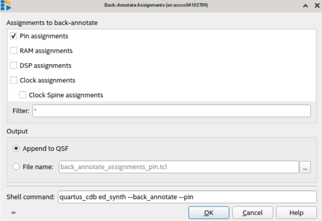
- In the pop-up window, select Pin Assignments.
- In the Output field, select Append to QSF. Click OK.
Figure 27. Back-Annotate Assignments Dialog Box
- Navigate to the Compilation dashboard, and click Compile Design.