External Memory Interfaces Agilex™ 7 M-Series FPGA IP User Guide
- 4.1.2. s0_axi4_clock_out for Agilex 7 M-Series External Memory Interfaces (EMIF) IP - DDR4 Component
- 4.3.2. s0_axi4_clock_out for Agilex 7 M-Series External Memory Interfaces (EMIF) IP - DDR5 Component
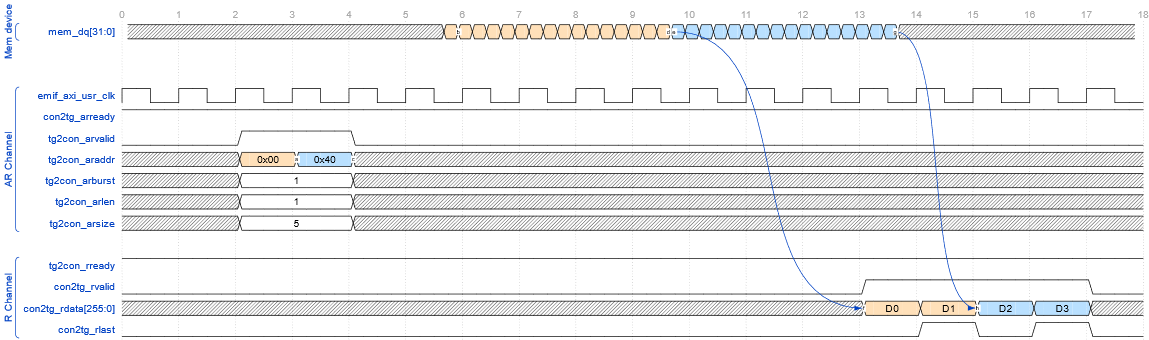
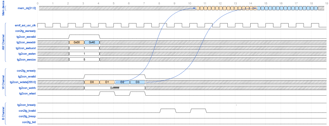
10.5.6. AXI Interface: Write and Read Example
In this context, "tg" refers to any AXI4 Master, while "con" represents the EMIF IP.
In the example, two separate transactions are initiated: the first targets address 0x00, and the second targets address 0x40. Each transaction consists of two transfers (with arlen=1, indicating a burst length of 2), and each transfer is 32 bytes in size (awsize=5) for a total of 64 bytes per transaction.
On the W channel, as indicated by the color coding in the diagram, D0 and D1 represent the two 32-byte (256-bit) transfers of the first transaction. The subsequent two transfers, shown in blue, correspond to the second transaction. The wlast signal marks the end of each transaction.
In this setup, the EMIF IP is connected to DDR5 memory, which expects 16 consecutive data packets of 32 bits for each access. To meet this requirement, the EMIF IP collects the incoming AXI data and rearranges the two transfers of each transaction into two bursts of 16 data packets. These rearranged bursts are also color-coded in the diagram below.
As in the previous example, the following diagram illustrates a read transaction accessing addresses 0x00 and 0x40. For each AXI4 read request, the EMIF IP issues a corresponding read command to the DDR5 memory device, which responds with a burst of 16 consecutive 32-bit data packets.
The EMIF IP collects this data and reorganizes it to be sent over the AXI4 R channel as two transactions, each composed of two 256-bit (32-byte) transfers. Each transfer is signaled on the R channel, and the end of each burst is indicated by the rlast signal. This process ensures that the data returned from DDR5 memory is properly formatted and aligned with AXI4 protocol requirements.