External Memory Interfaces Agilex™ 7 M-Series FPGA IP User Guide
ID
772538
Date
4/01/2024
Public
A newer version of this document is available. Customers should click here to go to the newest version.
1. About the External Memory Interfaces Agilex™ 7 M-Series FPGA IP
2. Agilex™ 7 M-Series FPGA EMIF IP – Introduction
3. Agilex™ 7 M-Series FPGA EMIF IP – Product Architecture
4. Agilex™ 7 M-Series FPGA EMIF IP – End-User Signals
5. Agilex™ 7 M-Series FPGA EMIF IP – Simulating Memory IP
6. Agilex™ 7 M-Series FPGA EMIF IP – DDR4 Support
7. Agilex™ 7 M-Series FPGA EMIF IP – DDR5 Support
8. Agilex™ 7 M-Series FPGA EMIF IP – LPDDR5 Support
9. Agilex™ 7 M-Series FPGA EMIF IP – Timing Closure
10. Agilex™ 7 M-Series FPGA EMIF IP – Controller Optimization
11. Agilex™ 7 M-Series FPGA EMIF IP – Debugging
12. Document Revision History for External Memory Interfaces Agilex™ 7 M-Series FPGA IP User Guide
3.1.1. Agilex™ 7 M-Series EMIF Architecture: I/O Subsystem
3.1.2. Agilex™ 7 M-Series EMIF Architecture: I/O SSM
3.1.3. Agilex™ 7 M-Series EMIF Architecture: I/O Bank
3.1.4. Agilex™ 7 M-Series EMIF Architecture: I/O Lane
3.1.5. Agilex™ 7 M-Series EMIF Architecture: Input DQS Clock Tree
3.1.6. Agilex™ 7 M-Series EMIF Architecture: PHY Clock Tree
3.1.7. Agilex™ 7 M-Series EMIF Architecture: PLL Reference Clock Networks
3.1.8. Agilex™ 7 M-Series EMIF Architecture: Clock Phase Alignment
3.1.9. User Clock in Different Core Access Modes
6.2.4.1. Address and Command Pin Placement for DDR4
6.2.4.2. DDR4 Data Width Mapping
6.2.4.3. General Guidelines - DDR4
6.2.4.4. x4 DIMM Implementation
6.2.4.5. Specific Pin Connection Requirements
6.2.4.6. Command and Address Signals
6.2.4.7. Clock Signals
6.2.4.8. Data, Data Strobes, DM/DBI, and Optional ECC Signals
6.3.5.1. Single Rank x 8 Discrete (Component) Topology
6.3.5.2. Single Rank x 16 Discrete (Component) Topology
6.3.5.3. ADDR/CMD Reference Voltage/RESET Signal Routing Guidelines for Single Rank x 8 and Single Rank x 16 Discrete (Component) Topologies
6.3.5.4. Skew Matching Guidelines for DDR4 Discrete Configurations
6.3.5.5. Power Delivery Recommendations for DDR4 Discrete Configurations
6.3.5.6. Agilex™ 7 M-Series EMIF Pin Swapping Guidelines
7.3.1. PCB Stack-up and Design Considerations
7.3.2. General Design Considerations
7.3.3. DDR Differential Signals Routing
7.3.4. Ground Plane and Return Path
7.3.5. RDIMM, UDIMM, and SODIMM Break-in Layout Guidelines
7.3.6. DRAM Break-in Layout Guidelines
7.3.7. DDR5 PCB Layout Guidelines
7.3.8. DDR5 Simulation Strategy
7.3.7.1. DDR5 Discrete Component/Memory Down Topology: up to 40-Bit Interface (1 Rank x8 or x16, 2 Rank x8 or x16)
7.3.7.2. Routing Guidelines for DDR5 Memory Down: 1 Rank or 2 Rank (x8 bit or x16 bit) Configurations
7.3.7.3. Routing Guidelines for DDR5 RDIMM, UDIMM, and SODIMM Configurations
7.3.7.4. Example of a DDR5 layout on Intel FPGA Platform Board
11.1. Interface Configuration Performance Issues
11.2. Functional Issue Evaluation
11.3. Timing Issue Characteristics
11.4. Verifying Memory IP Using the Signal Tap Logic Analyzer
11.5. Debugging with the External Memory Interface Debug Toolkit
11.6. Generating Traffic with the Test Engine IP
11.7. Guidelines for Developing HDL for Traffic Generator
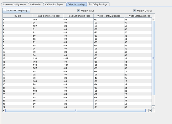
11.5.4.5. Driver Margining Tab
The driver margining feature lets you measure margins on your memory interface using a driver with predefined traffic patterns.
Margins measured with this feature are expected to be smaller than margins measured during calibration, because this traffic pattern is longer than those run during calibration, and is intended to stress the interface.
To use driver margining, press Run Driver Margining, at the top-left of the tab. The toolkit then measures margins for DQ read, DQ write, and DM. The process usually takes a few minutes, depending on the margin size, the interface size, and the duration of the driver tests.
The system displays the test results in the table when the test has completed.
Figure 80. Driver Margining Tab