Intel Agilex® 7 General-Purpose I/O User Guide: F-Series and I-Series
A newer version of this document is available. Customers should click here to go to the newest version.
2.5.8. External Memory Interface Pin Placement Requirements
Within a GPIO bank, the top sub-bank is located near the edge of the die while the bottom sub-bank is near the FPGA core.
Interconnects between the sub-banks chain the sub-banks into a row. The following figures show examples of how I/O lanes in various sub-banks are chained together to form the top and bottom I/O rows in different device variants. These figures represent the top view of the silicon die that corresponds to a reverse view of the device package.
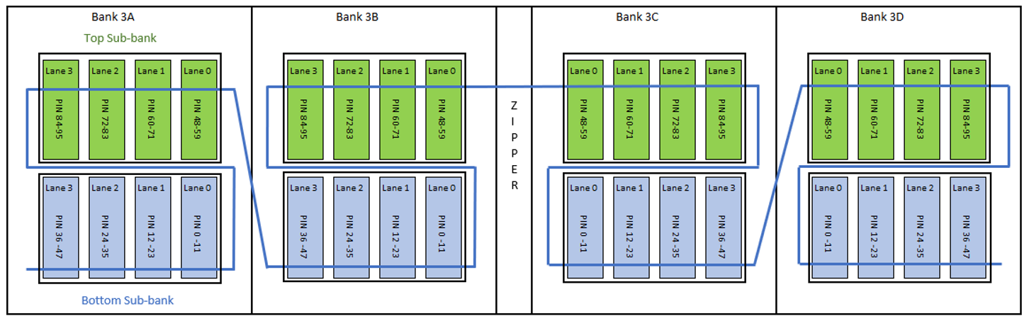
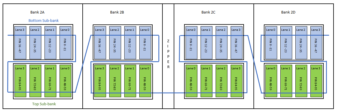
The two sub-banks within an I/O bank are adjacent to each other, unless any of the sub-banks is not bonded out or partially bonded out. The blue line in the figures shows the connectivity between the sub-banks.
For example, in the top row bank of the AGF 012 and AGF 014 devices:
- The top sub-bank in bank 3A is adjacent to the bottom sub-bank in bank 3A and the bottom sub-bank in bank 3B.
- The top sub-bank in bank 3B is adjacent to the bottom sub-bank in bank 3B and the top sub-bank in bank 3C.
- The top sub-bank in bank 3B is adjacent to the top sub-bank in bank 3C even though there is a zipper block between the two sub-banks.
- The top sub-bank in bank 3B is not adjacent to the bottom sub-bank in bank 3A.
You can identify where a pin is located within an I/O bank based on its Index within I/O Bank value in the device pinout file.