1.4. Simulating the Design Example
Figure 5. Procedure
- Change to the testbench simulation directory, pcie_example_design_tb.
- Run the simulation script for the simulator of your choice. Refer to the table below.
- Analyze the results.
| Simulator | Working Directory | Instructions |
|---|---|---|
| ModelSim* | <example_design>/pcie_example_design_tb/pcie_example_design_tb/sim/mentor/ |
|
| VCS* | <example_design>/pcie_example_design_tb/pcie_example_design_tb/sim/synopsys/vcs |
|
| NCSim* | <example_design>/pcie_example_design_tb/pcie_example_design_tb/sim/cadence |
|
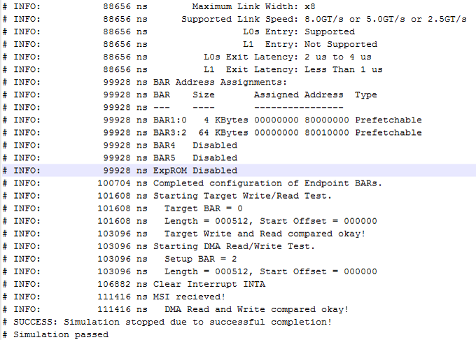
The simple DMA testbench completes the following tasks:
- Writes to the Endpoint memory using the DUT Endpoint Avalon® -MM RX master interface.
- Reads from Endpoint memory using the DUT Endpoint Avalon® -MM RX master interface.
- Verifies the data using the shmem_chk_ok task.
- Writes to the Endpoint DMA controller, instructing the DMA controller to perform a MemRd request to the PCIe* address space in host memory.
- Writes to the Endpoint DMA controller, instructing the DMA controller to perform a MemWr request to PCIe* address space in host memory. This MemWr uses the data from the previous MemRd.
- Verifies the data using the shmem_chk_ok task.
The simulation reports, "Simulation stopped due to successful completion" if no errors occur.
Figure 6. Partial Transcript from Successful Simulation Testbench