4.8. Intel® FPGA PTC - Clock Page
Intel® Agilex™ and Intel® Stratix® 10 devices support global, regional, and periphery clock networks. The Intel® FPGA PTC does not distinguish between global or regional clocks because the difference in power is not significant.
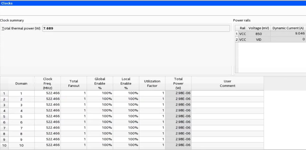
| Column Heading | Description |
|---|---|
| Domain | Enter a name for the clock domain in this column. This is an optional value. |
| Clock Freq (MHz) | Enter the frequency of the clock domain. This value is limited by the maximum frequency specification for the device family.
Note:
When you import a design from the Intel® Quartus® Prime software, some imported clocks may have a frequency of 0 MHz, due to either of the following reasons:
|
| Total Fanout | Enter the total number of flipflops, hyper-registers, RAMs, digital signal processing (DSP) blocks, and I/O pins fed by this clock. The number of resources driven by every global clock and regional clock signal is reported in the Fan-out column of the Intel® Quartus® Prime Compilation Report. In the Compilation Report, select Fitter and click Place Stage. Select Global & Other Fast Signals Summary and observe the Fan-out value.
Note: Power consumed by Intel® Stratix® 10 MLAB clocks is accounted for in the RAM page; therefore, clock fanout on this page does not include any MLABs driven by this clock domain, for Intel® Stratix® 10 devices. For Intel® Agilex™ devices, MLAB is included in the fanout.
|
| Global Enable % | Enter the average percentage of time that the entire clock tree is enabled. Each global clock buffer has an enable signal that you can use to dynamically shut down the entire clock tree. |
| Local Enable % | Enter the average percentage of time that clock enable is high for destination flipflops. Local clock enables for flipflops in ALMs are promoted to LAB-wide signals. When a given flipflop is disabled, the LAB-wide clock is disabled, cutting clock power and the power for down-stream logic. This page models only the impact on clock tree power. |
| Utilization Factor | Represents the impact of the clock network configuration on power. Characteristics that have a large impact on power and are captured by this factor include the following:
The default value for this field is typical; the actual value varies between clocks in your design, and depends on the placement of your design. For most accurate results, you should import this value from the Intel® Quartus® Prime software after compiling your design, because the Intel® Quartus® Prime software has access to detailed placement information. In the absence of an Intel® Quartus® Prime design, higher values generally correspond to signals that span large distances on the FPGA and fanout to many destinations, while lower values correspond to more localized signals. You can change this field from its default value to explore possible variations in power consumption depending on block placement. When changing this value, keep in mind that typical designs rarely use extreme values, and only for a small subset of the design. |
| Total Power (W) | Indicates the total power dissipation due to clock distribution (in W). |
| User Comments | Enter any comments. This is an optional entry. |
For more information about the clock networks of Intel® Agilex™ devices, refer to the Intel Agilex Clocking and PLL User Guide.