F-Tile Avalon® Streaming IP for PCI Express* Design Example User Guide
3.3.2.2.1. Configure the Testbench to Perform a Dword Address-Aligned Read and Write Operation
The simulation testbench from the Programmed Input/Output (PIO) design example can be modified to demonstrate Double Word (DW) address alignment through 16 iterations of Memory Write (MWr) and Memory Read (MRd) operations. The initial address is set to 0x00, with a payload size of 1 DW. In each iteration, both the Transaction Layer Packet (TLP) payload and the request address increment by 1 DW. The data retrieved from MRd operations are validated against the corresponding MWr data. Any mismatches identified during the comparison are logged as errors in the simulation logfile.
The waveform shows the increment of the address and payload size.
First iteration (address of 0000_0001_0000_0000, payload of 1DW)
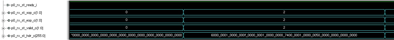
Second iteration (address of 0000_0001_0000_0004, payload of 2DW)

- Locate the file altpcietb_bfm_rp_gen4_x16.sv in the <design example directory>/pcie_ed_sim_tb/ip/pcie_ed_sim_tb/dut_pcie_tb_ip/intel_pcie_ftile_tbed_100/sim/ directory.
- Modify the following localparam in the altpcietb_bfm_rp_gen4_x16.sv file as shown below:
Line 6037: RCSLAVE_MAXLEN=16;
Note: The RCSLAVE_MAXLEN is to control the loop count of the MWr/MRd instruction routines. - Task downstream_read is responsible for the MWr/MRd instruction routines. It initiates the MWr and MRd based on the variable passed in.
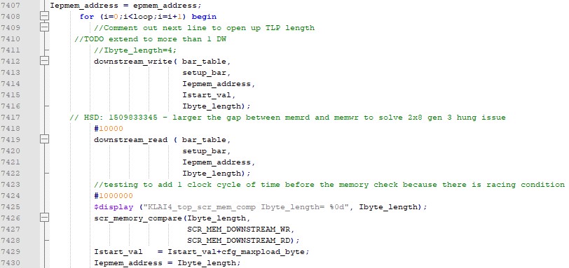
- Insert “Iepmem_address = epmem_address;” after line 7407.
- Comment out “Ibyte_length=4; at line 7411.
- Rename lines 7414 and 7421 from “epmem_address;” to “Iepmem_address,”.
- Uncomment line 7424 to enable a delay of #1000000.
- Insert “Iepmem_address = Ibyte_length;” after line 7429.
- The successful run should have 16 iterations of MWr and MRd. The logfile should contain the message “successful completion!”