F-Tile Interlaken Intel® FPGA IP Design Example User Guide
ID
683069
Date
1/14/2022
Public
A newer version of this document is available. Customers should click here to go to the newest version.
1.2. Generating the Design
Figure 3. Procedure
Follow these steps to generate the design example and testbench:
- In the Intel® Quartus® Prime Pro Edition software, click File > New Project Wizard to create a new Intel® Quartus® Prime project, or click File > Open Project to open an existing Intel® Quartus® Prime project. The wizard prompts you to specify a device.
- Specify the device family Agilex and select device with F-Tile for your design.
- In the IP Catalog, locate and double-click F-Tile Interlaken Intel FPGA IP. The New IP Variant window appears.
- Specify a top-level name <your_ip> for your custom IP variation. The parameter editor saves the IP variation settings in a file named <your_ip>.ip.
- Click OK. The parameter editor appears.
Figure 4. Example Design Tab
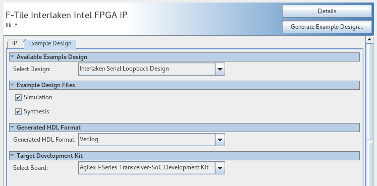
- On the IP tab, specify the parameters for your IP core variation.
- On the Example Design tab, select the Simulation option to generate the testbench. Select the Synthesis option to generate the hardware design example. You must select at least one of the Simulation and Synthesis options to generate the design example.
- For Generated HDL Format, both Verilog and VHDL option is available.
- For Target Development Kit, select the Agilex I-Series Transceiver-SOC Development Kit.
Note: When you select the Development Kit option, the pin assignments are set according to the Intel® Agilex™ I-Series Transceiver-SoC Development Kit device part number (AGIB027R31B1E2VR0) and may differ from your selected device. If you intend to test the design on hardware on a different PCB, select No development kit option and make the appropriate pin assignments in the .qsf file
- Click Generate Example Design. The Select Example Design Directory window appears.
- If you want to modify the design example directory path or name from the defaults displayed (ilk_f_0_example_design), browse to the new path and type the new design example directory name.
- Click OK.
Note: In the F-Tile Interlaken Intel FPGA IP design example, a SystemPLL is instantiated automatically, and connected to F-Tile Interlaken Intel FPGA IP core. The SystemPLL hierarchy path in the design example is:
example_design.test_env_inst.test_dut.dut.pll