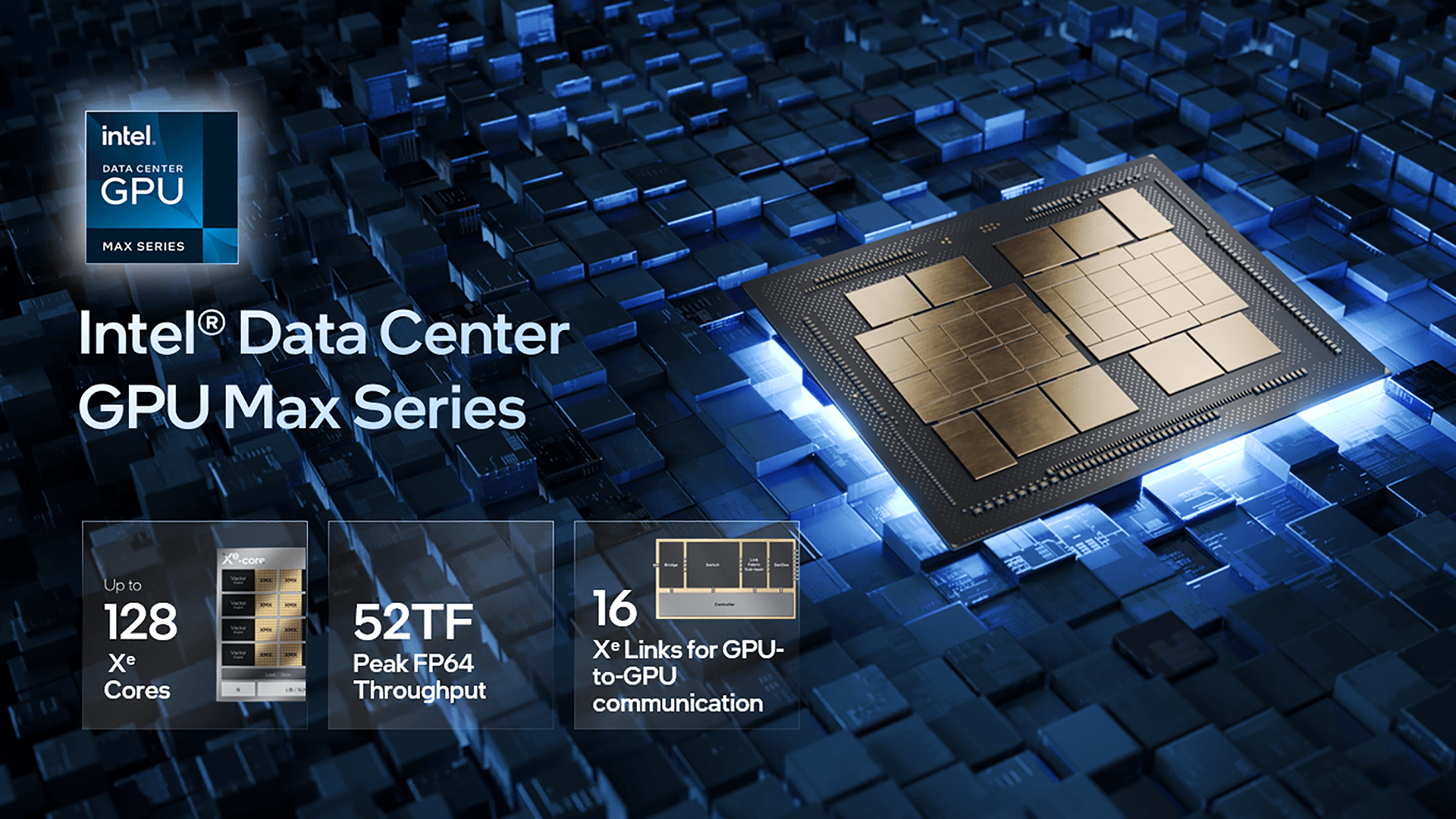
This article discusses the capabilities available in the Intel® Data Center GPU Max Series previously codename Ponte Vecchio and how developers can take advantage of them. This new GPU product is based on the Intel Xe HPC micro-architecture. The GPU uses highly parallelized computing models associated with AI and HPC. It is supported by the oneAPI open ecosystem with the flexibility of Single Instruction Multiple Data (SIMD) and Single Instruction Multiple Threads (SIMT).
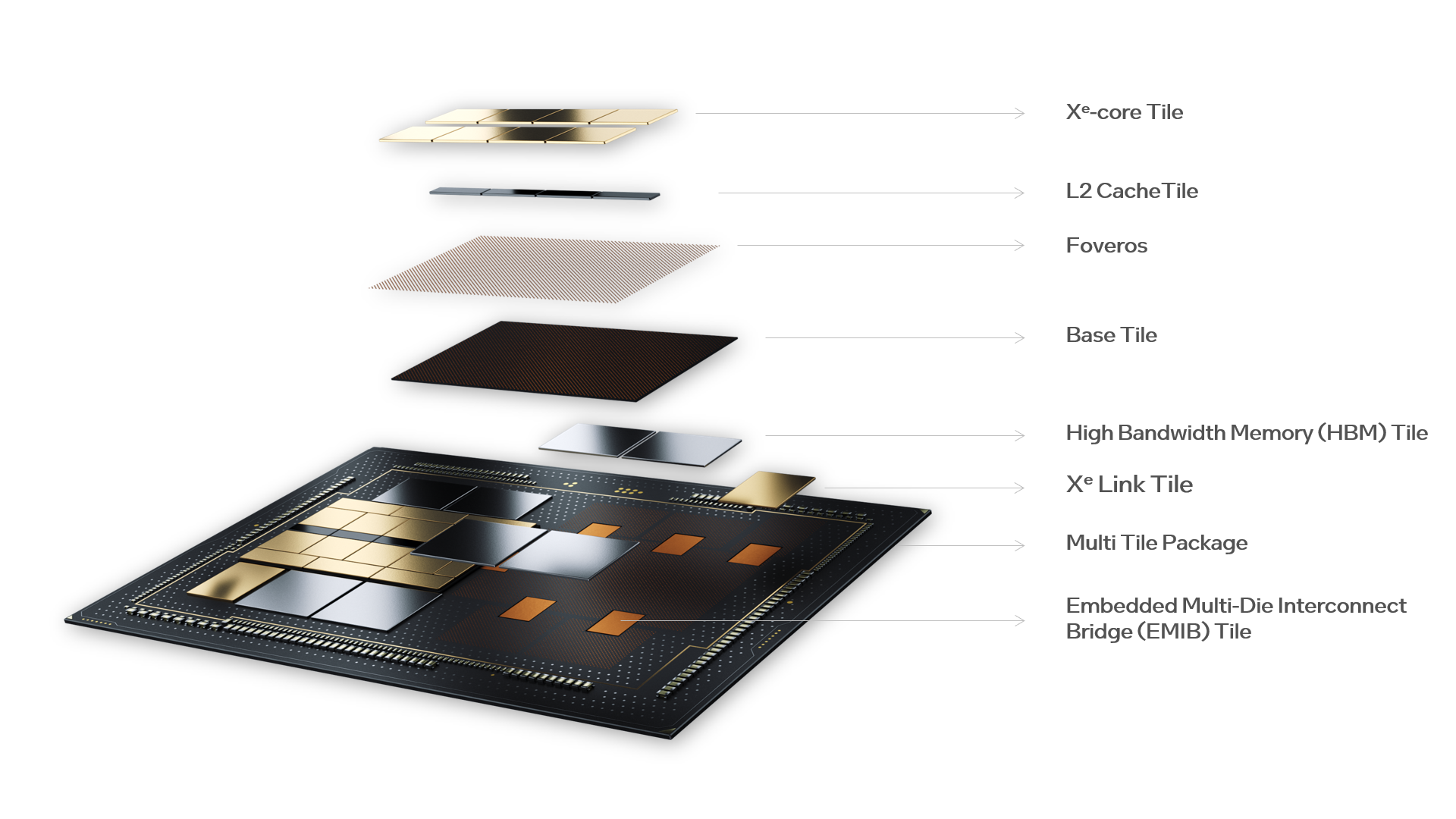
Figure 1 – High level Xe HPC Stack Component Overview
At the heart of the product is the Xe HPC Stack, which is comprised of various tiles stacked upon each other within a single package. The components of the Xe HPC Stack are comprised of the Xe-core Tile (Compute Tile), L2 Cache Tile, Base Tile (PCIe paths, media engine, copy engine, etc.), High Memory Bandwidth Tile, Xe Link Tile for scale-up and scale-out, and the Embedded Multi-Die Interconnect Bridge (EMIB) for communication between Xe HPC Stacks. These components all reside within a Multi Tile Package.
Intel Xe HPC Micro-Architecture
Over the course of this article, we are going to cover the different functional aspects of the total solution. This includes a discussion of the architecture, multiple execution units are combined into an individual core, multiple cores are combined into a slice, multiple slices are combined into a stack and multiple stacks are incorporated into different form factors to become different product lines.
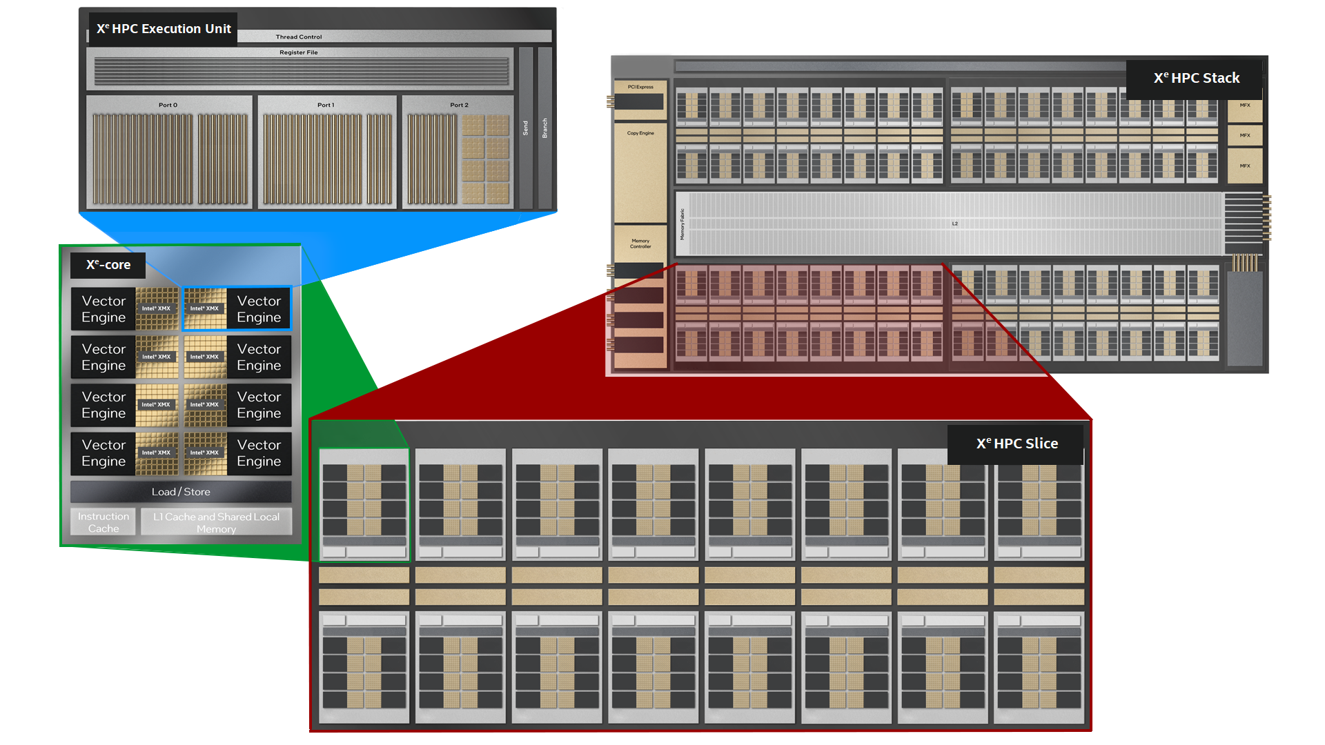
Figure 2 – Block Diagram Of The different components of the Intel Xe HPC Micro-Architecture
Intel Xe is a scalable graphics and compute architecture designed to deliver exceptional performance and functionality. The product includes a discrete PCIe add-in card and an OpenCompute Accelerator Module (OAM) to provide solutions that require increased GPU density within the data center. Intel’s Xe Architecture consists of one of three possible micro-architectures: Xe LP a low-power solution, Xe HPG which is optimized for enthusiasts and gaming, or Xe HPC which is optimized for HPC and AI acceleration. Intel® Data Center GPU Max Series is built upon the Xe HPC micro-architecture with a compute focused, programable and scalable element called the Xe-core. This Xe-core is made up of a combination of Vector Engines, Matrix engines that are referred to in this article as Intel® Xe Matrix Extensions (Intel® XMX), cache and shared local memory. Each Xe-core contains eight 512-bit Vector Engines designed to accelerate traditional graphics, compute, and HPC workloads. Along with eight 4096-bit Intel XMX, engineered to accelerate AI workloads. The Xe-core provides 512KB of L1 cache and shared local memory to support the engines.
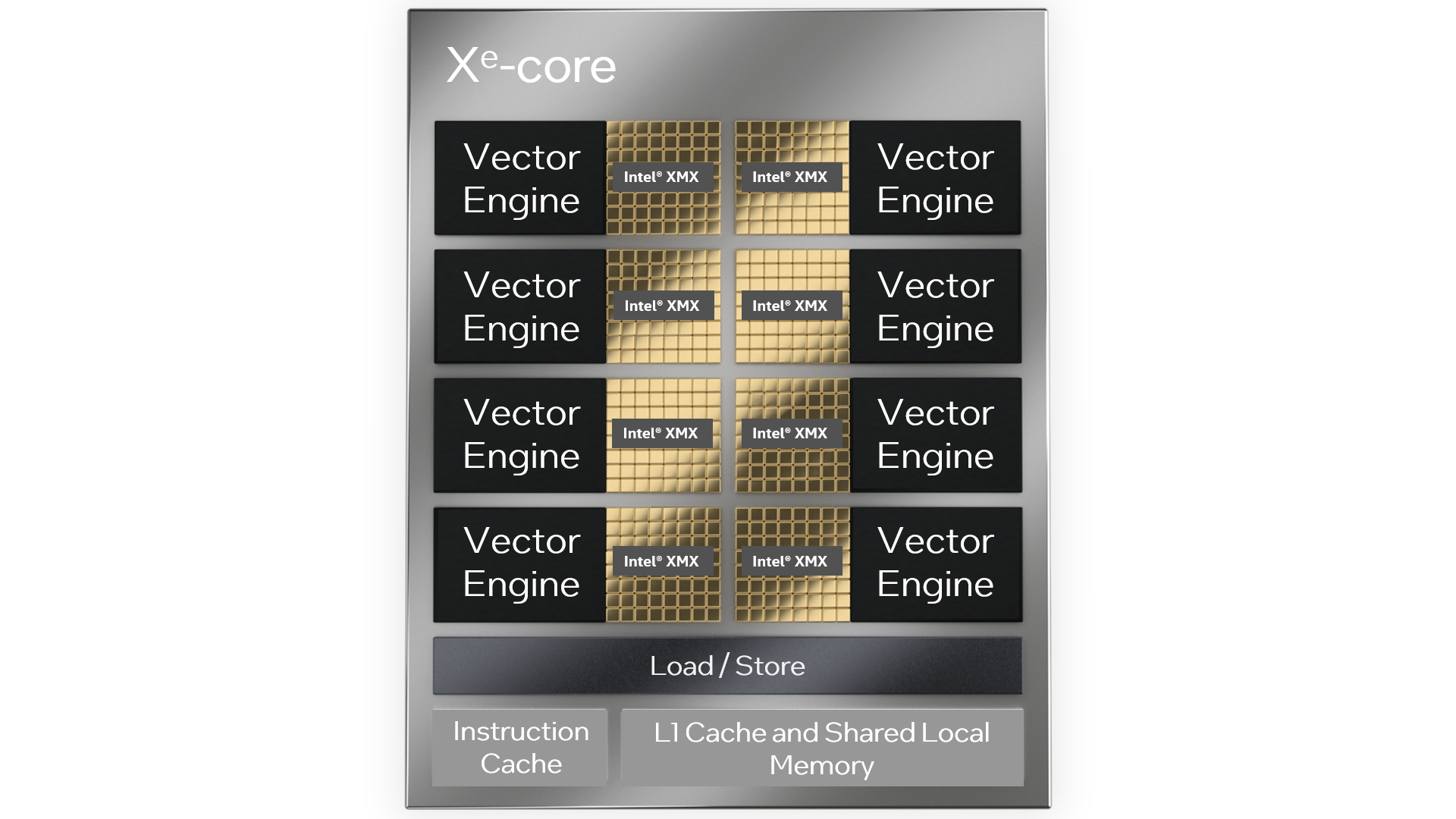
Figure 3 – Xe-core Block Diagram With Xe HPC Micro-Architecture
Developers can optimize their software for use with the Xe HPC micro-architecture by using libraries and compilers that leverage the instruction set architecture (ISA). This will take advantage of the ports previously referred to as the Data Parallel Matrix Engine. Within one of the execution units of the Xe-core can be found three ports that support a variety of programming data types to help maximize application performance. The Xe-core has eight vector engines with a 512-bit wide register supporting all “vector” or non-systolic numerics as follows, FP64 (256 ops per clock), FP32 (256 ops per clock), and FP16 (512 ops per clock). While the Intel XMX systolic array depth has been increased to 8 as compared to an Xe HPG Core providing 4096-bits for each of the units. Intel XMX supports systolic numerics as follows, TF32 (2048 ops per clock), FP16 (4096 ops per clock), BF16 (4096 ops per clock) and Int8 (8192 ops per clock). New data types introduced to support specific segments include a 64-bit double precision float (FP64) to benefit HPC workloads utilizing the Vector Engines. A 32-bit tensor float (TF32) data type is provided to benefit AI workloads using Intel XMX. The L1 data cache and shared local memory have been increased to help support the additional flops introduced by these new data types. The load/store unit has also been enhanced for nd-tensor data structures.
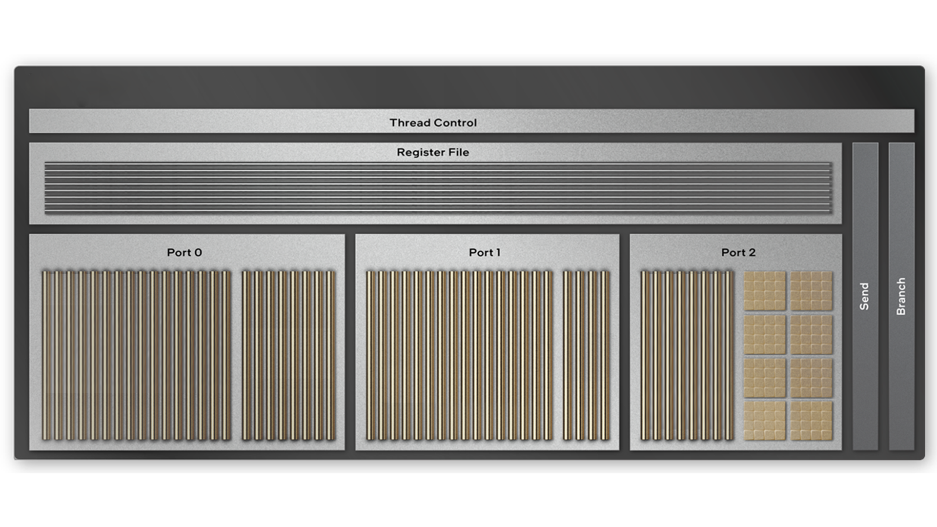
Figure 4 – Inside one of the execution units of the Xe-core on the Xe HPC micro-architecture
The operations supplied to an execution unit of the Xe HPC micro-architecture will be serviced by one of the three ports. Integer and floating-point operations are separated out into two separate ports to increase throughput by running calculations parallel. The port architecture allows AI applications, matrix operations, element-wise vector operations and address computations to all be executed concurrently. If broader HPC applications require higher precision, the dual-issued double precision pipes deliver FP64 vector compute at 1x rate as compared to FP32.
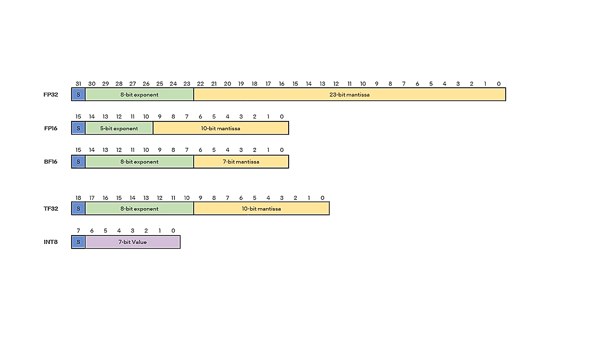
Figure 5 – Data Type Comparison
Deep Neural Networks have a high tolerance to numerical precisions. Comparing the different data types, higher system performance with AI workloads can be achieved with lower and mixed precision operations. The 32-bit floating-point format (FP32) is the default for deep learning training and inference. When we look at what the other data types offer as compared to FP32 we can see their advantages. The 32-bit tensor float (TF32) data type, which can be enabled with a simple global setting, reduces the precision (only 10 bits mantissa) with the same 8-bit exponent. Because of this the throughput for TF32 is higher than FP32 just based on the amount of work done per clock cycle. The 16-bit floating-point format (FP16) can do more work per clock cycle than TF32 due to a 5-bit exponent, but it requires special handling techniques via loss scaling. The Brain Floating Point Format (BF16) is also a 16-bit floating point data type. It matches the dynamic range of FP32 and TF32 with an 8-bit exponent while having a lower precision than either, with only 7-bits of mantissa. It doesn’t suffer from the special handling required by FP16 yet is able to match its throughput advantage making it ideal for training as compared to FP32, FP16 or TF32. The 8-bit integer (INT8) data type can be used for post-training quantization for faster inference. This is due to its smaller 8-bit size as compared to FP32, FP16, BF16, or TF32 reducing both the memory and computing requirements. Even though it is faster it lacks the precision of the other data types, which only makes it useful for inference instead of training. Cloud edge devices involved with deep learning, which have smaller memory and bandwidth requirements is an area that can benefit from INT8.
Due to the general-purpose nature of the execution unit, it can process both Single Instruction Multiple Data (SIMD) and Single Instruction Multiple Threads (SIMT). Typically, SIMD is used by CPUs while SIMT is used by GPUs. The execution unit provides parallelism for both the thread and data elements. Software developers can benefit from the parallel nature of the data by extending the parallelism of the instructions. Simultaneously executing both SIMT and SIMD provides a unique opportunity for potential performance improvements. OneAPI presents an opportunity for ease of development with this approach.
Xe HPC Slice
Building up from the Xe-cores to create a functional SoC (System on a Chip) infrastructure we start with the Xe HPC Slice. It is comprised of sixteen Xe-cores combined with sixteen ray tracing units along with a hardware context. The ray tracing units provide fixed-function computation for Ray Traversal Bounding Box Intersection, and Triangle Intersection. The hardware context enables execution of multiple applications concurrently without expensive software-based context switches.
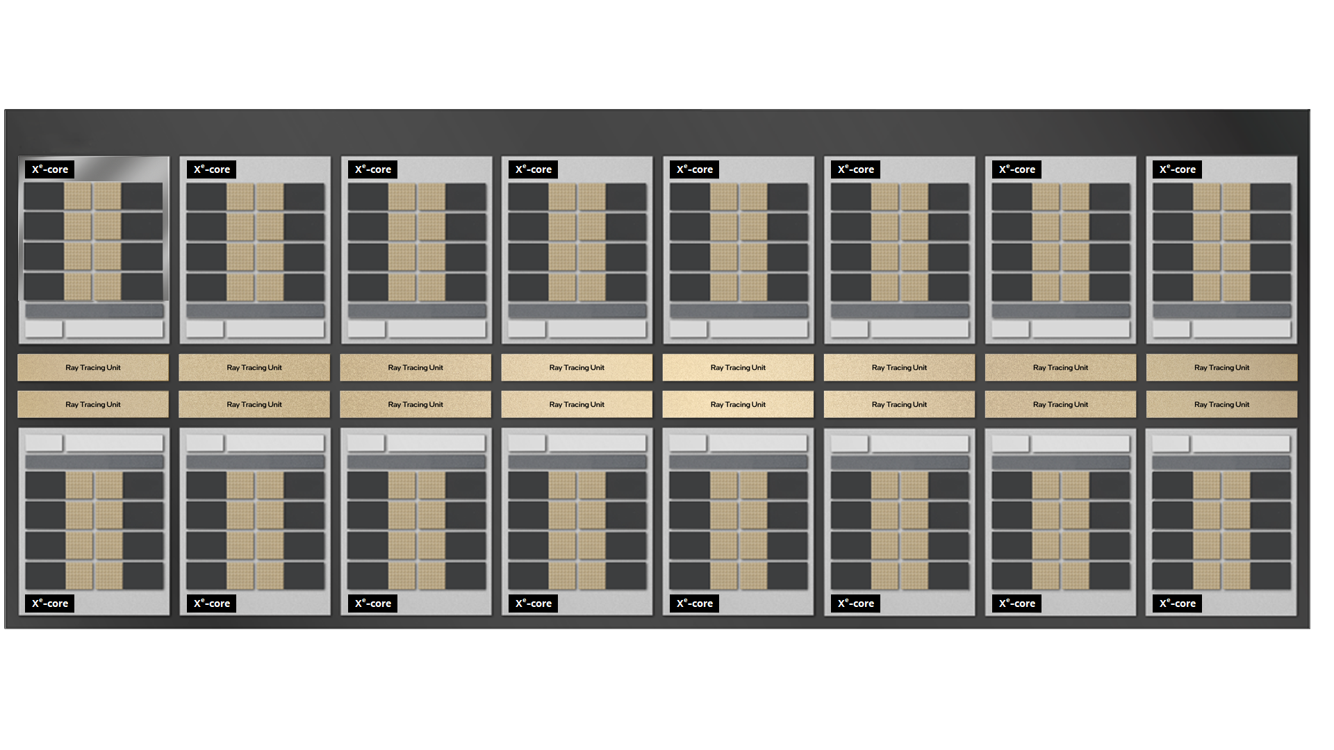
Figure 6 – Xe HPC Slice
Xe HPC Stack
Four Xe HPC Slices are then combined with an L2 cache, one media engine, Gen 5 PCI Express interconnect, a memory controller, and eight Xe Links to form an Xe HPC Stack. The L2 cache can be up to a size of 204MB, the media engine performs decode only functions for AVC, AVI and HEVC. In a two-stack configuration the communication occurs via the Embedded Multi-Die Interconnect Bridge (EMIB) interface with up to 230 GB/s in both directions. The Xe Links provide a high-speed coherent unified fabric for communications between GPUs to support scale up and scale out.
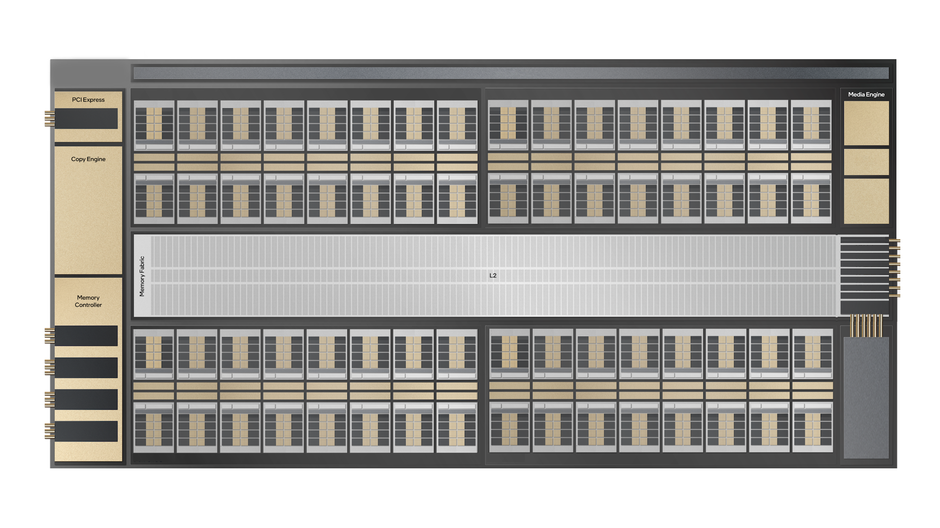
Figure 7 – Xe HPC Stack
From a perspective of form factor a single Xe HPC Stack can be used to create a PCIe add-in card. While more than one Xe HPC Stack can be combined within a physical package also known as an OpenCompute Accelerator Module (OAM). The OAM’s are placed onto a carrier baseboard for scalability and the sled can be plugged into a server via PCI Express.
Xe Link
The Xe Link is designed to provide a high-speed coherent unified fabric for communications between the Xe HPC Stacks. This includes both the internal communication within an OAM as well as across multiple OAMs. It supports load and store operations, bulk data transfers and synchronization of semantics. The technology is a scalability feature that can provide communications for up to eight Xe HPC Stacks (x8 Glueless) via an embedded switch. Each Xe Link is capable of up to 26.5 GB/s of bandwidth in each direction.
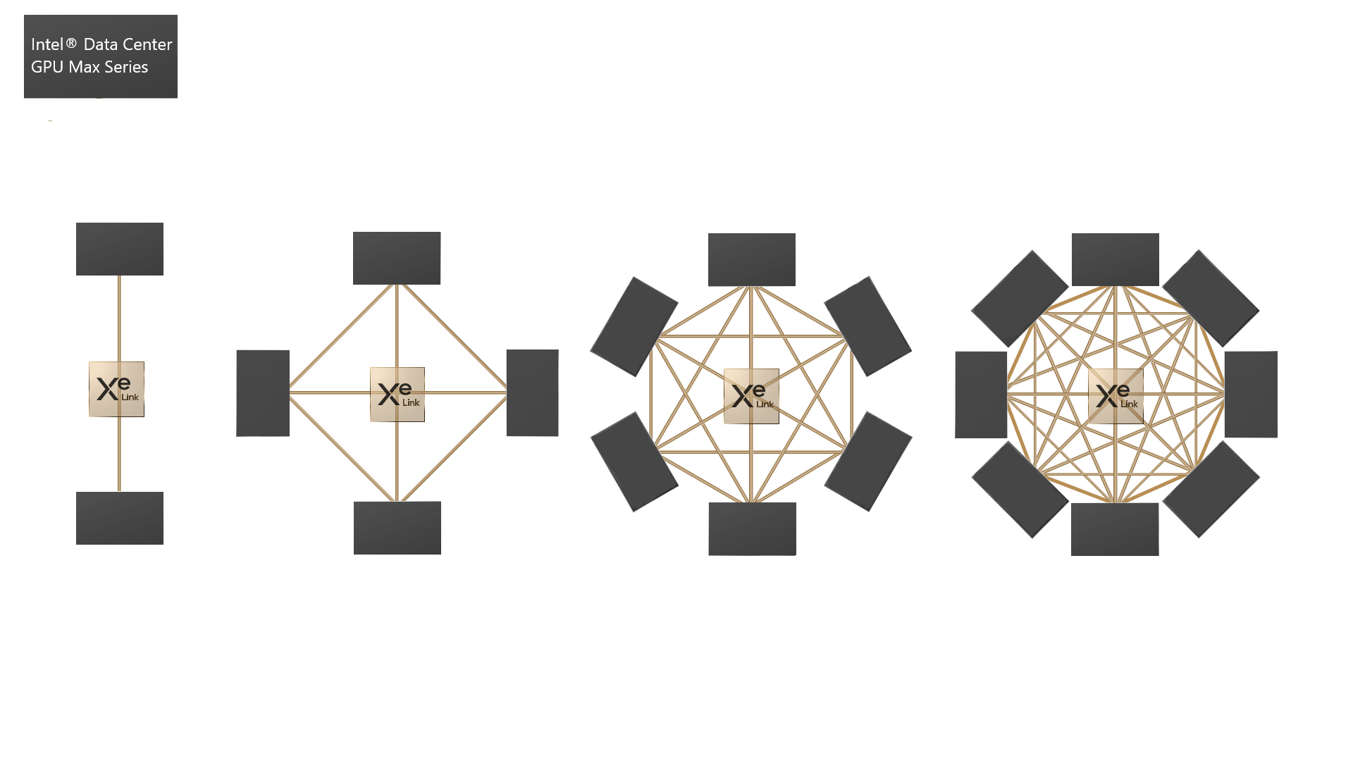
Figure 8 - Xe Link Configuration Options
Scale Up
The Xe Link is integral to scale up and scale out solutions. The expansion of the number of Xe HPC Stacks instances within a single system is known as a scale up solution. This can take on different configurations depending on whether PCI express cards are used or OAMs. A PCI Express card has a single Xe HPC Stack and six Xe Links available for scaling up. The supported PCI Express card configurations would be a two-card configuration with six Xe Links between each Xe HPC Stack. The second supported configuration would be four PCI Express cards with two Xe Links between each Xe HPC Stack. With a bandwidth of 26.6 GB/s in each direction per Xe Link this means that in a two-card configuration the bandwidth would be 159 GB/s in each direction and in a four card configuration the bandwidth would be 53 GB/s in each direction. Figure 8 shows varying levels of Xe Link connectivity that is possible with different amounts of PCI Express cards and OAMs. Ease of use for developers on scale up solutions is provided by the OS kernel. The kernel provides access to all the execution units without any needing any code changes.
Scale Out
A scale out solution is when you need to connect multiple nodes together to create a larger cluster of execution units. Up to a maximum of sixty-four interconnected OAMs can be linked together using a single form of external communication between the nodes. The inter-node communication can be a NIC-based solution using an InfiniBand fabric. Alternatively, an Xe Link Glueless solution using directly connected passive copper cables can be utilized to achieve linking together sixty-four OAMs. A need for scaling out beyond sixty-four OAMs can be accomplished by combining Xe Link Glueless along with a NIC-based InfiniBand fabric. This combination can provide up to 512 inter-connected OAMs.
Intel’s initial offering will be a carrier base board that contains four OAMs to create a half width sled. This configuration codenamed Tuscany can be plugged into an existing server via the Gen 5 PCI Express bus. It provides a high-density solution for use with HPC workloads. There will be options for a 450 watt and a 600 watt versions that can support liquid or air cooled systems on single or dual processor systems. PCI Express add in cards will be available in addition to the OAMs. The table below gives an overview of the different product specifications.
Micro-Architecture Overview
Table 1. Intel® Data Center GPU Max Series Micro-Architecture Overview
|
|
Specifications below are per OAM. Note that in the case of Intel’s product offering on a half width sled, codenamed Tuscany there will be four OAMs. |
PCI Express Card |
|
|---|---|---|---|
|
SKU |
OAM SKU Based on a Thermal Design Power of 600 Watts |
OAM SKU Based on a Thermal Design Power of 450 Watts |
PCI Express Card with a Thermal Design Power of 300 Watts |
|
Thermal Design Power |
600 watts – Liquid cooling only |
450 watts – Liquid or Air cooling |
300 watts – Air cooling only |
|
Silicon |
Xe-core (Codename Ponte Vecchio) |
Xe-core (Codename Ponte Vecchio) |
Xe-core (Codename Ponte Vecchio) |
|
Xe HPC Stacks |
Two Xe HPC Stacks |
Two Xe HPC Stacks |
One Xe HPC Stack |
|
Xe HPC Micro-Architecture |
128 Xe-cores with a total of 1024 Vector Engines and 1024 Matrix Engines |
96 Xe-cores with a total of 896 Vector Engines and 896 Matrix Engines |
56 Xe-cores with a total of 448 Vector Engines and 448 Matrix Engines |
|
L1 Cache |
64MB total or 512KB per Xe-core |
48MB total or 512KB per Xe-core |
28MB total or 512KB per Xe-core |
|
L2 Cache |
408MB total or 204MB per Xe HPC Stack (ECC support is this associated with L2 or something else?) |
216MB total or 108MB per Xe HPC Stack (ECC support is this associated with L2 or something else?) |
108MB total (ECC support is this associated with L2 or something else?) |
|
Memory |
128GB HBM2e total or 64GB per Xe HPC Stack with an aggregate bandwidth of 12.8 TB/s |
96GB HBM2e total or 48GB per Xe HPC Stack with an aggregate bandwidth of 12.8 TB/s |
48MB total or 512KB per Xe-core with an aggregate bandwidth of 12.8 TB/s |
|
Embedded Multi-Die Interconnect Bridge (EMIB) Interface |
230 GB/s between Xe HPC Stacks 1 and 2 within the same OAM |
230 GB/s between Xe HPC Stacks 1 and 2 within the same OAM |
N/A |
|
Xe Links |
16 total or 8 per Xe HPC Stack Each link is capable of 26.5 GB/s of bandwidth in each direction |
16 total or 8 per Xe HPC Stack Each link is capable of 26.5 GB/s of bandwidth in each direction |
3 total supporting x2 or x4 bridge Each link is capable of 26.5 GB/s of bandwidth in each direction |
|
HBM |
Up to 4x HBM2e 3.2GT/s |
Up to 4x HBM2e 3.2GT/s |
Up to 4x HBM2e 3.2GT/s |
|
Memory Capacity |
16G-128G (1T to 2T) Dedicated |
||
|
PCI Express |
Gen5 |
Gen5 |
Gen5 |
|
PCIe |
X16 PCIe Gen5 per tile |
||
|
Media Codec Support |
Decode only functions for AVC, AVI and HEVC |
Decode only functions for AVC, AVI and HEVC |
Decode only functions for AVC, AVI and HEVC |
|
FP64 PEAK FLOPS |
52 TFLOPS |
44 TFLOPS |
22 TFLOPS |
|
FP32 PEAK FLOPS |
52 TFLOPS |
44 TFLOPS |
22 TFLOPS |
|
BF16 PEAK FLOPS |
832 TFLOPS |
704 TFLOPS |
352 TFLOPS |
|
INT8 PEAK FLOPS |
1664 TFLOPS |
1408 TFLOPS |
704 TFLOPS |
Virtualization
The Xe HPC micro-architecture supports virtualization built upon Single Root I/O Virtualization (SR-IOV). Sixty-three virtual functions (VFs) are possible with a two Xe HPC Stack implementation to help with the scalability of virtualization. To assist with management VF profiles can be dynamically modified without taking the system offline. Additionally, there is flexibility to administer both heterogeneous or homogeneous profiles across the device or tile. Security of the VFs is done through both hardware isolation of the device and at the Xe HPC Stack. Isolating the data within the memory associated with device and at the Xe HPC Stack provides an additional level of security.
Virtualization can be implemented at the OAM level (i.e. multiple Xe HPC Stacks) or at the individual Xe HPC Stack level. The entire OAM’s processing and memory capabilities can be dedicated to a single virtual function or each Xe HPC Stack within the OAM can be associated with a separate VF. Alternatively, VFs can share the entire OAM or an Xe HPC Stack via an allotted a slice of time. These modes of operation are managed by the hypervisor and provide full memory isolation between the VFs.
Software
Intel oneAPI is provided for ease of adoption for software developers and includes a complete set of advanced compliers, libraries, and a code migration with SYCL along with analysis and debugger tools. Developers can be confident that existing applications will work seamlessly with oneAPI due to its interoperability with existing programming models and code bases (C++, Fortran, Python, OpenMP, etc.). The transition to CPUs, GPUs, FPGAs, and AI accelerators using a single code base in Data Parallel C++ helps to optimize a developer’s time. A good place to begin for application developers is the workflow guide focused on the GPU and the Intel® oneAPI Base Toolkit.
The Intel oneAPI Base Toolkit provides a set of high-performance tools for building C++ and Data Parallel C++ applications. While domain specific toolkits are available for specific workloads. Intel oneAPI Tools for HPC provides support for scalability of Fortran, OpenMP and MPI applications. Intel oneAPI Tools for IoT is designed to help developers that are designing solutions at the edge of the network. Intel oneAPI AI Analytics Toolkit provides support for optimization of Deep Learning frameworks and Python libraries to assist with machine learning and data science pipelines. Intel oneAPI Rendering Toolkit focuses on visualization applications. Intel Distribution of OpenVINO Toolkit assists developers working with inference and applications from the edge to the cloud. Lastly for guidance on code optimization see the oneAPI GPU Optimization Guide.
If you are focused on AI and work with PyTorch or the Tensor Flow Frameworks, the latest versions are compatible with the Intel® Data Center GPU Max Series.
Additional Resources:
Technical Overview Of The Intel® Xeon® Scalable processor Max Series
Technical Overview Of The 4th Gen Intel® Xeon® Scalable processor family
Code Sample: Intel® Advanced Matrix Extensions (Intel® AMX) - Intrinsics Functions
Intel® In-Memory Analytics Accelerator (Intel® IAA) Enabling Guide
Proof Points of Intel® Dynamic Load Balancer (Intel® DLB)
The Author: David Mulnix is a software engineer and has been with Intel Corporation for over 20 years. His areas of focus include technical content development and training, software automation, server performance and power analysis with SPECPower, and he supported the development effort for the Server Efficiency Rating ToolTM.
Notices/Disclaimers
Performance varies by use, configuration and other factors. Learn more on the Performance Index site.
No product or component can be absolutely secure.
Code names are used by Intel to identify products, technologies, or services that are in development and not publicly available. These are not "commercial" names and not intended to function as trademarks
Intel disclaims all express and implied warranties, including without limitation, the implied warranties of merchantability, fitness for a particular purpose, and non-infringement, as well as any warranty arising from course of performance, course of dealing, or usage in trade
Your costs and results may vary.
Intel technologies may require enabled hardware, software or service activation.
© Intel Corporation. Intel, the Intel logo, and other Intel marks are trademarks of Intel Corporation or its subsidiaries. Other names and brands may be claimed as the property of others.