AXI Streaming Intel® FPGA IP for PCI Express* User Guide
ID
790711
Date
1/24/2025
Public
1. Introduction
2. Features
3. Getting Started with the AXI Streaming Intel® FPGA IP for PCI Express*
4. IP Architecture and Functional Description
5. AXI Streaming Intel® FPGA IP for PCI Express* Parameters
6. Interfaces and Signals
7. Register Descriptions
8. Document Revision History for the AXI Streaming Intel® FPGA IP for PCI Express* User Guide
A. Specifications
B. Simulating the Design Example
1.1. Goal of the AXI Streaming Intel® FPGA IP for PCI Express* User Guide
1.2. Intended Audience for the AXI Streaming Intel® FPGA IP for PCI Express* User Guide
1.3. What is PCI Express* ?
1.4. What are the Intel® FPGA IPs for PCI Express* ?
1.5. What is the AXI Streaming Intel® FPGA IP for PCI Express* ?
1.6. Example Use Models
1.7. Design Flow Requirements
3.1. Download and Install Quartus Software
3.2. Obtain and Install Intel FPGA IPs and Licenses
3.3. Configure and Generate the AXI Streaming Intel® FPGA IP for PCI Express*
3.4. About the AXI Streaming Intel® FPGA IP for PCI Express Design Examples
3.5. Instantiate and Connect the AXI Streaming Intel® FPGA IP for PCI Express* Interfaces
3.6. Simulate the AXI Streaming Intel® FPGA IP for PCI Express* IP Variant
3.7. Compile the AXI Streaming Intel® FPGA IP for PCI Express* IP Variant
3.8. Software Drivers for AXI Streaming Intel® FPGA IP for PCI Express* IP Variant
3.9. Build the Application for the AXI Streaming Intel® FPGA IP for PCI Express* IP Variant
3.10. Verification with the AXI Streaming Intel® FPGA IP for PCI Express* IP Variant
3.11. Debugging with the AXI Streaming Intel® FPGA IP for PCI Express* IP Variant
4.1. Clocks and Resets
4.2. PCIe Hard IP (HIP)
4.3. HIP Interface (IF) Adaptor
4.4. Application Error Reporting
4.5. Debug Toolkit and Hard IP (HIP) Reconfiguration Interface
4.6. Configuration Space Extension
4.7. Control Shadow
4.8. Configuration Intercept Interface
4.9. Power Management
4.10. Legacy Interrupt
4.11. Credit Handling
4.12. Completion Timeout
4.13. Transaction Ordering
4.14. Page Request Service (PRS) Events
4.15. TX Non-Posted Metering Requirement on Application
4.16. MSI Pending
4.17. D-State Status
4.18. Configuration Retry Status Enable
4.19. AXI-Streaming Interface
4.20. Precision Time Measurement (PTM)
6.1. Overview
6.2. Clocks and Resets
6.3. Application Packet Interface
6.4. Configuration Extension Bus Interface
6.5. Configuration Intercept Interface
6.6. Function Level Reset Interface
6.7. Control Shadow Interface (st_ctrlshadow)
6.8. Completion Timeout Interface (st_cplto)
6.9. Miscellaneous Signals
6.10. Control and Status Register Responder Interface (lite_csr)
6.11. Error Interface (st_err)
6.12. VF Error Flag Interface (vf_err/sent_vfnonfatalmsg)
6.13. VIRTIO PCI* Configuration Access Interface
6.14. Serial Data Signals
7.3.1.1. AXI Streaming Intel® FPGA IP for PCI Express* Version
7.3.1.2. AXI Streaming Intel® FPGA IP for PCI Express* Features
7.3.1.3. AXI Streaming Intel® FPGA IP for PCI Express* Interface Attributes
7.3.1.4. HOT PLUG GEN CTRL
7.3.1.5. POWER MANAGEMENT CTRL
7.3.1.6. LEGACY INTERRUPT CTRL
7.3.1.7. CFG REG IA CTRL
7.3.1.8. CFG REG IA FN NUM
7.3.1.9. CFG REG IA WRDATA
7.3.1.10. CFG REG IA RDDATA
7.3.1.11. PRS CTRL
7.3.1.12. MSI PENDING CTRL
7.3.1.13. MSI PENDING
7.3.1.14. D-STATE STS
7.3.1.15. CFG RETRY CTRL
7.3.3.1. PERFMON CTRL
7.3.3.2. TX MRD TLP
7.3.3.3. TX MWR TLP
7.3.3.4. TX MSG TLP
7.3.3.5. TX CFGWR TLP
7.3.3.6. TX CFGRD TLP
7.3.3.7. RX MRD TLP
7.3.3.8. RX MWR TLP
7.3.3.9. RX MSG TLP
7.3.3.10. RX CFGWR TLP
7.3.3.11. RX CFGRD TLP
7.3.3.12. TX MEM DATA
7.3.3.13. TX CPL DATA
7.3.3.14. RX MEM DATA
7.3.3.15. RX CPL DATA
3.4.1. Functional Description for the Programmed Input/Output (PIO) Design Example
The Programmed Input/Output (PIO) design example performs memory transfers from a host processor to a target device. In this design example, the host processor performs Memory Read (MemRd) and Memory Write (MemWr) Transaction Layer Packets (TLPs). Note that this design example does not support back-to-back transactions from the host processor since the design is intended to showcase single-dword transactions.
The PIO design example automatically creates the files necessary to simulate and compile in the Quartus® Prime software. The design example covers a wide range of parameters. However, it does not cover all possible parameterizations of the AXI Streaming IP for PCI Express.
This design example supports the following configurations:
| Port Mode | Link Width | Link Speed | HIP Data Width (Bits) | Application Data Width (Bits) | Compact/HIP Native Mode | Design Example Support |
|---|---|---|---|---|---|---|
| Endpoint | 1x16 | Gen5 | 1024 (4 x 256) | 1024 (4 x 256) | HIP Native | SCTH |
| 2x8 | Gen5 | 512 (2 x 256) | 512 (2 x 256) | HIP Native | SCTH | |
| Root Port | N/A | N/A | N/A | N/A | N/A | N/A |
| TL Bypass | N/A | N/A | N/A | N/A | N/A | N/A |
Note: The R-Tile AXI Streaming PIO design example only supports VCSMX (Verilog) and Questasim (Verilog/VHDL) for simulation.
Figure 8. PIO AXI Streaming 1x16, 1x8, 1x4 Design Example Block Diagram

Note: 1x4 is not supported in this release.
Figure 9. PIO AXI Streaming 2x8, 2x4 Design Example Block Diagram
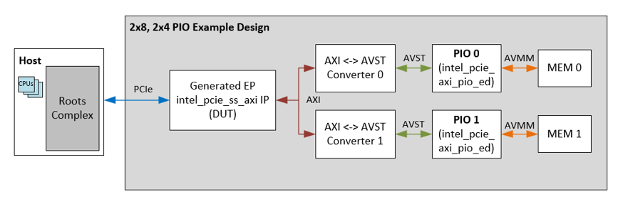
Note: 2x4 is not supported in this release.