High Bandwidth Memory (HBM2E) Interface Intel Agilex® 7 M-Series FPGA IP Design Example User Guide
A newer version of this document is available. Customers should click here to go to the newest version.
2.5.1. High Bandwidth Memory (HBM2E) Interface Intel® FPGA IP Example Design For Simulation
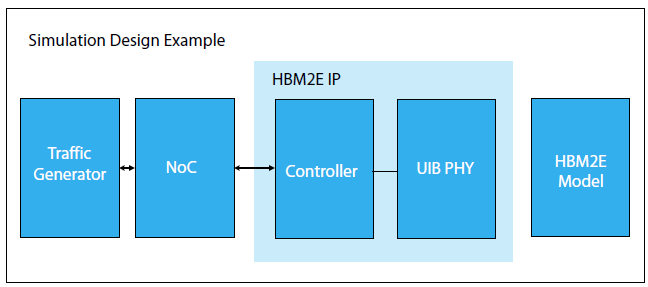
The Traffic Generator emulates a real-world application that writes to, and reads back from memory and validates the read data. You can modify the traffic generator traffic pattern or drive the transactions to the HBM2E memory with your own logic.
Simulation incorporates abstract models of the NoC and HBM2E memory device. The hardened HBM2E controller is simulated in full, and simulation of the UIB is simplified by omitting the calibration phase. The HBM2E controller converts AXI memory access commands to HBM commands. The universal interface block PHY (UIB PHY) is the physical-layer interface that carries low-level signaling between the controller and HBM2E device.
The HBM2E Model is an abstract generic model representative of the HBM2E DRAM for simulation. This is not a vendor-specific model.