A newer version of this document is available. Customers should click here to go to the newest version.
1. About the Nios® V Embedded Processor
2. Nios® V Processor Hardware System Design with Intel® Quartus® Prime Software and Platform Designer
3. Nios® V Processor Software System Design
4. Nios® V Processor Configuration and Booting Solutions
5. Nios® V Processor - Using the MicroC/TCP-IP Stack
6. Nios® V Processor Debugging, Verifying, and Simulating
7. Nios® V Processor — Remote System Update
8. Nios® V Processor — Using Custom Instruction
9. Nios® V Embedded Processor Design Handbook Archives
10. Document Revision History for the Nios® V Embedded Processor Design Handbook
4.1. Introduction
4.2. Linking Applications
4.3. Nios® V Processor Booting Methods
4.4. Introduction to Nios® V Processor Booting Methods
4.5. Nios® V Processor Booting from Configuration QSPI Flash
4.6. Nios V Processor Booting from On-Chip Memory (OCRAM)
4.7. Summary of Nios® V Processor Vector Configuration and BSP Settings
6.4.1. Prerequisites
6.4.2. Setting Up and Generating Your Simulation Environment in Platform Designer
6.4.3. Creating Nios V Processor Software
6.4.4. Generating Memory Initialization File
6.4.5. Generating System Simulation Files
6.4.6. Running Simulation in the QuestaSim Simulator Using Command Line
4.5.1.1.1. Hardware Design Flow
The following sections describe the steps for building a bootable system for a Nios® V processor application, which executes in place from the configuration QSPI flash.
The following example is built using an Intel Arria 10 SoC Development Kit.
IP Component Settings
- Create your Nios® V processor project using Intel® Quartus® Prime and Platform Designer.
- Add Generic Serial Flash Interface Intel FPGA IP into your Platform Designer.
Figure 17. Connections for Nios® V Processor ProjectFigure 18. Generic Serial Flash Interface Intel FPGA IP Parameter Settings
- Change the Device Density (Mb) according to the QSPI flash size.
- Change the addressing mode by modifying bit 8 of the Control Register value in the Default Settings parameter section. Changing bit 8 to 0x0 enables 3-byte addressing, or 0x1 enables 4-byte addressing.
Note: Refer to Intel Supported Configuration Devices tab > Intel Supported Third Party Configuration Devices in the Device Configuration Support Center to check the byte addressing mode supported for each flash device in each Intel FPGA device.
For example, Intel® Arria® 10 devices support the 4-byte addressing mode when used with Micron flash devices .
Reset Agent Settings for Nios® V Processor Execute-In-Place Method
- In the Nios® V processor IP parameter editor, set the Reset Agent to QSPI Flash.
- Your (.sof) image size influences your reset offset configuration. The reset offset is the start address of the HEX file in QSPI flash and it must point to a location after the (.sof) image. If the (.sof) image space and the reset offset location overlap, Intel® Quartus® Prime software displays an overlap error. You can determine the minimum reset offset by using the configuration bitstream size from the device datasheet.
Refer to the following example:
- The uncompressed configuration bitstream size for Intel® Arria® 10 GX 660 is 252,959,072 bits (31,619,884 bytes).
- If the SOF image starts at address 0x0, the SOF image can extend up to address 0x1E27B2C. In this case, the minimum reset offset you can select to avoid overlap errors is 0x1E27B30.
- Intel recommends you to use a flash sector boundary address for the reset offset. Doing so allows you to update the application software image at a later time without interfering with the FPGA image.
Figure 19. Parameter Editor Settings
- Your (.sof) image size influences your reset offset configuration. The reset offset is the start address of the HEX file in QSPI flash and it must point to a location after the (.sof) image. If the (.sof) image space and the reset offset location overlap, Intel® Quartus® Prime software displays an overlap error. You can determine the minimum reset offset by using the configuration bitstream size from the device datasheet.
- Click Generate HDL, the Generation dialog box appears.
- Specify output file generation options and then click Generate.
Intel Quartus Prime Software Settings
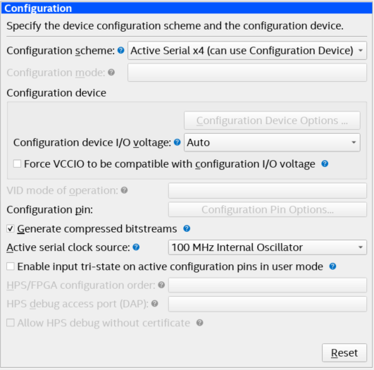
- In the Intel Quartus Prime software, click Assignment > Device > Device and Pin Options > Configuration.
- Set Configuration scheme to Active Serial x4 (can use Configuration Device).
- Set the Active serial clock source to 100 MHz Internal Oscillator.
Figure 20. Device and Pin Options
- Click OK to exit the Device and Pin Options window.
- Click OK to exit the Device window.
- Click Start Compilation to compile your project.
Related Information