A newer version of this document is available. Customers should click here to go to the newest version.
1. About the Nios® V Embedded Processor
2. Nios® V Processor Hardware System Design with Intel® Quartus® Prime Software and Platform Designer
3. Nios® V Processor Software System Design
4. Nios® V Processor Configuration and Booting Solutions
5. Nios® V Processor - Using the MicroC/TCP-IP Stack
6. Nios® V Processor Debugging, Verifying, and Simulating
7. Nios® V Processor — Remote System Update
8. Nios® V Embedded Processor Design Handbook Archives
9. Document Revision History for the Nios® V Embedded Processor Design Handbook
4.1. Introduction
4.2. Linking Applications
4.3. Nios® V Processor Booting Methods
4.4. Introduction to Nios® V Processor Booting Methods
4.5. Nios® V Processor Booting from Configuration QSPI Flash
4.6. Nios V Processor Booting from On-Chip Memory (OCRAM)
4.7. Summary of Nios® V Processor Vector Configuration and BSP Settings
6.4.1. Prerequisites
6.4.2. Setting Up and Generating Your Simulation Environment in Platform Designer
6.4.3. Creating Nios V Processor Software
6.4.4. Generating Memory Initialization File
6.4.5. Generating System Simulation Files
6.4.6. Running Simulation in the QuestaSim Simulator Using Command Line
4.5.1.2.1. Hardware Design Flow
The following sections describe a step-by-step method for building a bootable system for a Nios V processor application copied from configuration QSPI flash to RAM using GSFI Bootloader. The following example is built using Intel Arria 10 SoC Development Kit.
IP Component Settings
- Create your Nios® V processor project using Intel® Quartus® Prime and Platform Designer.
- Add the Generic Serial Flash Interface Intel FPGA IP is into your Platform Designer system.
Figure 33. Connections for Nios V Processor ProjectFigure 34. Generic Serial Flash Interface Intel FPGA IP Parameter Settings
- Change the Device Density (Mb) according to the QSPI flash size.
- Change the addressing mode by modifying bit 8 of the Control Register value in the Default Settings parameter section. Changing bit 8 to 0x0 enables 3-byte addressing, or 0x1 enables 4-byte addressing
Note: Refer to Intel Supported Configuration Devices tab > Intel Supported Third Party Configuration Devices in Device Configuration Support Center to check the byte addressing mode supported for each flash device in each Intel FPGA device.
For example, Intel® Arria® 10 devices when used with Micron flash devices support the 4-byte addressing mode.
Reset Agent Settings for Nios® V Processor Boot-copier Method
- In the Nios® V processor parameter editor, set the Reset Agent to QSPI Flash.
Figure 35. Nios V Parameter Editor Settings
- Click Generate HDL, the Generation dialog box appears.
- Specify output file generation options and then click Generate.
Intel Quartus Prime Software Settings
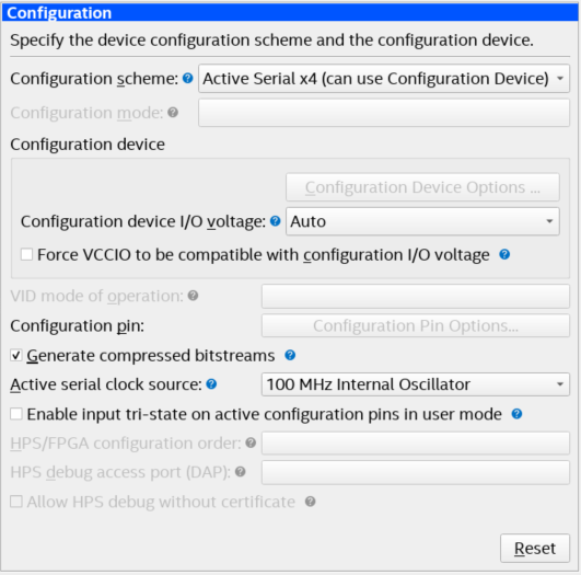
- In the Intel Quartus Prime software, click Assignment > Device > Device and Pin Options > Configuration .
- Set Configuration scheme to Active Serial x4 (can use Configuration Device).
- Set the Active serial clock source to 100 MHz Internal Oscillator.
Figure 36. Device and Pin Options
- Click OK to exit the Device and Pin Options window.
- Click OK to exit the Device window.
- Click Start Compilation to compile your project.
Related Information