1.2. Hardware Setup
Figure 1. Intel® Arria® 10 GX FPGA Development Kit Hardware SetupAn Intel® Arria® 10 GX FPGA Development Kit is used with the ADI AD9691 daughter card module installed to the development board’s FMC connector.
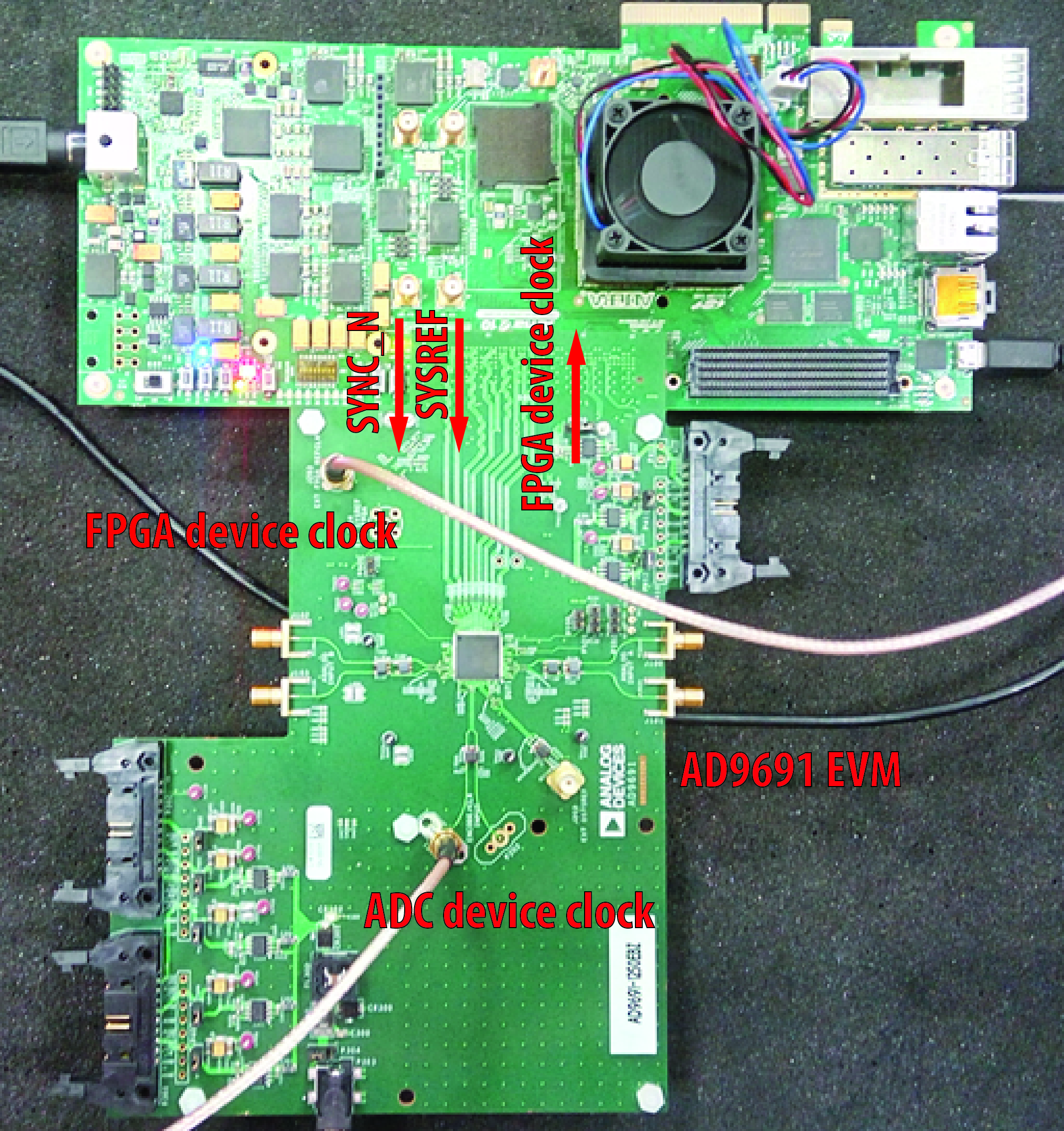
- The AD9691 EVM derives power from 4.5V power adaptor.
- The FPGA and ADC device clock is supplied by external clock source card through SMA connectors on AD9691 EVM.
- Both FPGA and ADC device clock must be sourced from the same clock source card with two different frequencies, one for FPGA and one for ADC.
For subclass 1, FPGA generates SYSREF for the JESD204B IP as well as the AD9691 device.
The following system-level diagram shows how the different modules connect in this design.
Figure 2. System Diagram
Note: The IOPLL input reference clock is sourcing from device clock through the global clock network. Sourcing reference clock from a cascaded PLL output, global clock or core clock network might introduce additional jitter to the IOPLL and transceiver PLL output. Refer to this KDB Answer for a workaround you should apply to the IP core in your design.
In this setup, where LMF=222, the data rate of transceiver lanes is 12.5 Gbps. An external clock source card provides 312.5 MHz clock to the FPGA and 625 MHz sampling clock to AD9691 device. The Sysref is generated by the FPGA.