R-tile Avalon® Streaming Intel® FPGA IP for PCI Express* Design Example User Guide
A newer version of this document is available. Customers should click here to go to the newest version.
1. About the R-tile Avalon® Streaming Intel® FPGA IP for PCI Express PIO Design Example
| Updated for: |
|---|
| Intel® Quartus® Prime Design Suite 22.1 |
| IP Version 5.0.0 |
The Programmed Input/Output (PIO) design example performs memory transfers from a host processor to a target device. In this example, the host processor requests single-dword Memory Read (MemRd) and Memory Write (MemWr) Transaction Layer Packets (TLPs).
The PIO design example automatically creates the files necessary to simulate and compile in the Intel® Quartus® Prime software. The design example covers a wide range of parameters. However, it does not cover all possible parameterizations of the R-tile Hard IP for PCIe.
This design example supports the following configurations:
| Port Mode | Link Width | Lin Speed | Data Width (Bits) | Design Example Support | Simulators Supported |
|---|---|---|---|---|---|
| Endpoint | x16 | Gen5 | 1024 (4 x 256) | SCTH (*) | Siemens EDA QuestaSim*, VCS*, VCS* MX |
| Gen4 | 1024 (4 x 256) | SCTH (*) | Siemens EDA QuestaSim*, VCS*, VCS* MX | ||
| 512 (2 x 256) | N/A | N/A | |||
| Gen3 | 1024 (4 x 256) | SCTH (*) | Siemens EDA QuestaSim*, VCS*, VCS* MX | ||
| 512 (2 x 256) | N/A | N/A | |||
| x8 | Gen5 | 512 (2 x 256) | SCTH (*) | Siemens EDA QuestaSim*, VCS*, VCS* MX | |
| Gen4 | 512 (2 x 256) | SCTH (*) | Siemens EDA QuestaSim*, VCS*, VCS* MX | ||
| 256 (1 x 256) | N/A | N/A | |||
| Gen3 | 512 (2 x 256) | SCTH (*) | Siemens EDA QuestaSim*, VCS*, VCS* MX | ||
| 256 (1 x 256) | N/A | N/A | |||
| x4 | Gen5 | 256 (2 x 128) | N/A | N/A | |
| Gen4 | 256 (2 x 128) | N/A | N/A | ||
| 128 (1 x 128) | N/A | N/A | |||
| Gen3 | 256 (2 x 128) | N/A | N/A | ||
| 128 (1 x 128) | N/A | N/A | |||
| Root Port | N/A | N/A | N/A | N/A | N/A |
| TLP Bypass | N/A | N/A | N/A | N/A | N/A |
| PIPE-D | N/A | N/A | N/A | N/A | N/A |
The clock is provided from the coreclkout_hip output of the IP and runs at 500 MHz.
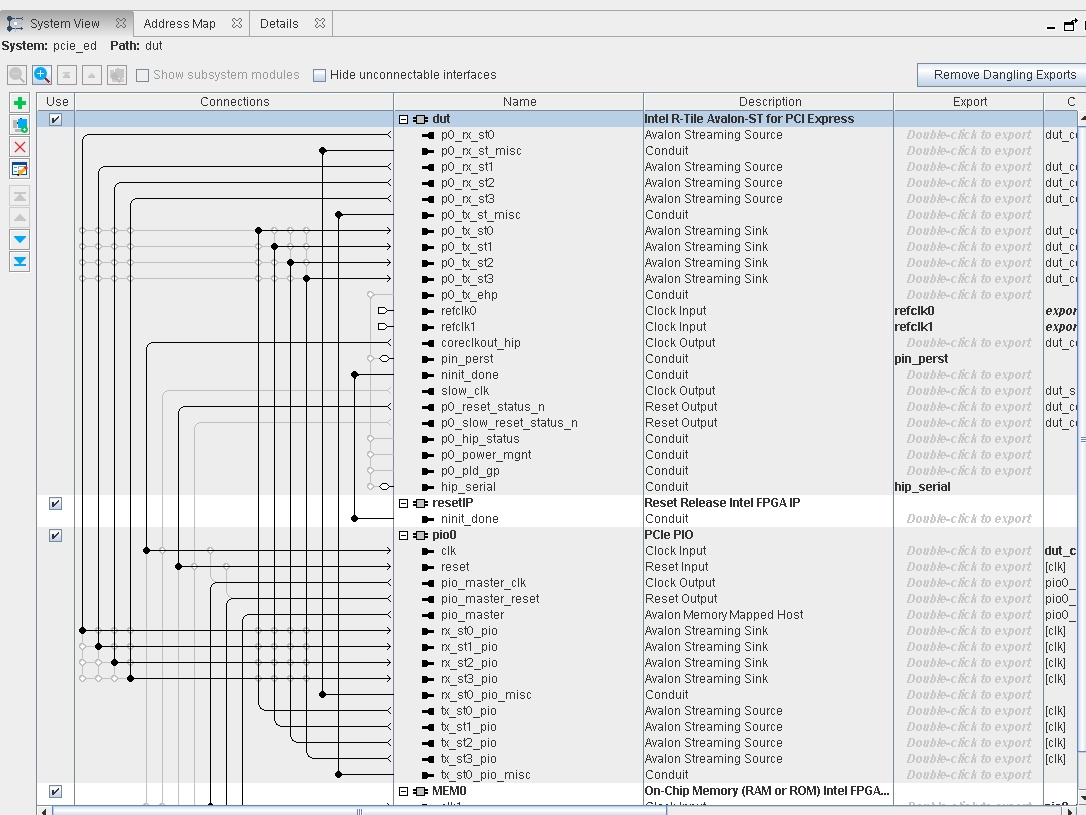
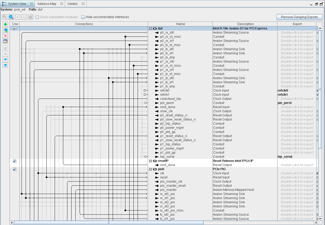
- The generated R-tile Avalon® Streaming (Avalon-ST) Hard IP Endpoint variant (DUT) with the parameters you specified. This component drives TLP data received to the PIO application. It translates the PCIe serial data received from the link to the Avalon® -ST data format.
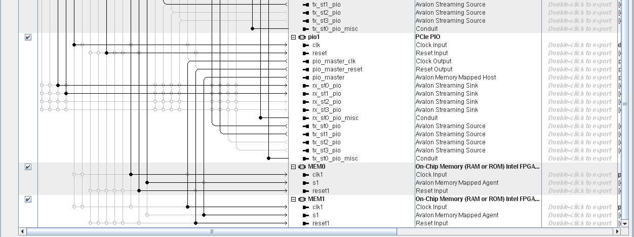
- The PIO Application (APPS) component, which performs the necessary translation between the PCI Express TLPs and simple Avalon® Memory-mapped ( Avalon® -MM) writes and reads to the on-chip memory.
Note: The current APPS component supports only single-cycle data transfers. Data transfers longer than one clock cycle are not supported.
- An on-chip memory (MEM) component (one 32 KB memory for the x16 design example, and two 32 KB memories for the 2x8 design example).
- Reset Release IP: This IP holds the control circuit in reset until the device has fully entered user mode. The FPGA asserts the nINIT_DONE output to signal that the device is in user mode. The nINIT_DONE signal is high until the entire device enters user mode. After nINIT_DONE deasserts (low), all logic is in user mode and operates normally.
In the Gen5 x16 design example, a PIO component with a 1024-bit data path is instantiated to interface with the 1024-bit DUT. Also, only one MEM device is instantiated as shown in the figure below.
In the Gen5 2x8 design example, two PIO components with 512-bit data paths are instantiated to interface with the 2x512-bit DUT. Also, two MEM devices are instantiated as shown in the figure below.
For simulation purposes, this design example also generates a testbench that instantiates the PIO design example and a Root Port BFM to interface with the target Endpoint.
The test program writes to and reads back data from the same location in the on-chip memory. It compares the data read to the expected result. The test reports, "Simulation stopped due to successful completion" if no errors occur.