F-Tile Avalon® Streaming Intel® FPGA IP for PCI Express* Design Example User Guide
A newer version of this document is available. Customers should click here to go to the newest version.
3.3.2.2. PIO Design Example Testbench
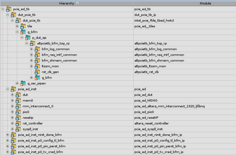
The figure below shows the PIO design example simulation design hierarchy. The tests for the PIO design example are defined with the apps_type_hwtcl parameter set to 3. The tests run under this parameter value are defined in ebfm_cfg_rp_ep_rootport, find_mem_bar and downstream_loop.
- Issue a memory write command to write a single dword of data into the on-chip memory behind the Endpoint.
- Issue a memory read command to read back data from the on-chip memory.
- Compare the read data with the write data. If they match, the test counts this as a Pass.
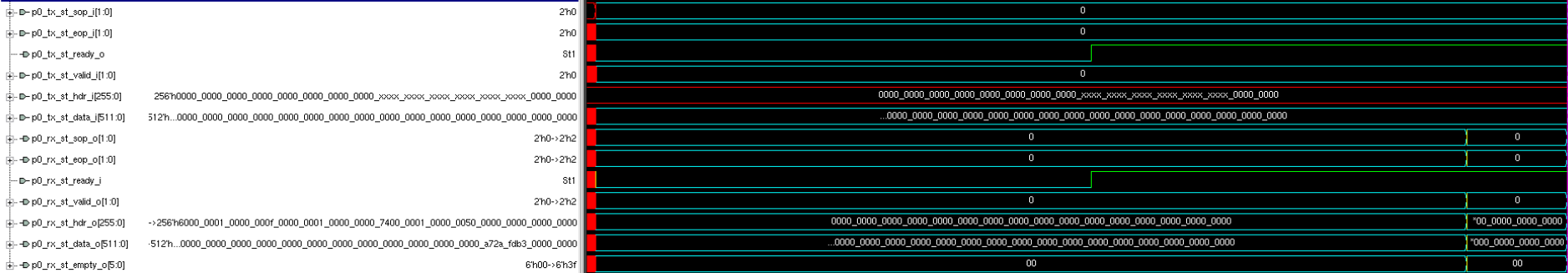
Trace the transition of signal p0_rx_st_sop_o[0] (for example h'0 to h'1) for the first memory write. It is followed by a memory read at the Avalon® -ST RX interface of the F-tile Hard IP for PCIe. The Completion TLP appears shortly after the memory read request at the Avalon® -ST TX interface. The memory write and read transactions and the Completion TLP are shown in the following waveforms.