Hyperflex® Architecture High-Performance Design Handbook
2.4.2.6. Read-Modify-Write Memory
Hyperflex® architecture FPGA M20K memory blocks support coherent reads to simplify implementing read-modify-write memory. Read-modify-write memory is useful in applications such as networking statistics counters. Read-modify-write memory is also useful in any application that stores a value in memory, that requires incrementing and re-writing in a single cycle.
M20K memory blocks simplify implementation by eliminating any need for hand-written caching circuitry. Caching circuitry that pipelines the modify operation over multiple clock cycles becomes complex because of high clock speeds or large counters.
To use the coherent read feature, connect memory according to whether you register the output data port. If you register the output data port, add two register stages to the write enable and write address lines when you instantiate the memory.
If you do not register the output data port, add one register stage to the write enable and write address lines when you instantiate the memory.
Use of coherent read has the following restrictions:
- Must use the same clock for reading and writing.
- Must use the same width for read and write ports.
- Cannot use ECC.
- Cannot use byte enable.
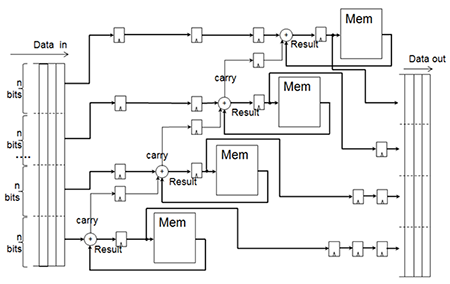
Pipelining Read-Modify-Write Memory shows a pipelining method for a read-modify-write memory that improves performance, without maintaining a cache for tracking recent activity.
If you require M20K memory features that are incompatible with coherent read, or if you do not want to use coherent read, use the following alternative approaches to improve the fMAX performance of memory:
- Break the modification operation into smaller blocks that can complete in one clock cycle.
- Ensure that each chunk is no wider than one M20K memory block. The Compiler splits data words into multiple n-bit chunks, where each chunk is small enough for efficient processing in one clock cycle.
- To increase fMAX, increase the number of memory blocks, use narrower memory blocks, and increase the latency. To decrease latency, use fewer and wider memory blocks, and remove pipeline stages appropriately. A loop in a read-modify-write circuit is unavoidable because of the nature of the circuit, but the loop in this solution is small and short. This solution is scalable, because the underlying structure remains the same regardless of the number of pipeline stages.