JESD204B Intel® Cyclone® 10 GX FPGA IP Design Example User Guide
ID
683298
Date
7/29/2024
Public
1.2.5.1. Platform Designer System Component
The Platform Designer system instantiates the JESD204B IP core data path and supporting peripherals.
Figure 8. Platform Designer System for System Console Control Design Example
The top level Platform Designer system instantiates the following modules:
- Platform Designer system
- JESD204B subsystem
- JTAG to Avalon® master bridge
- Parallel I/O (PIO)
- ATX PLL
- Core PLL
- Serial Port Interface (SPI)—master module
The following are the key features of the top level Platform Designer system:
- Supports System Console control design example
- Supports 3 data path types:
- Duplex—Both TX and RX data paths present
- Simplex TX—Only TX data path present
- Simplex RX—Only RX data path present
- Supports transceiver dynamic reconfiguration enabled mode:
- When enabled, connects the JTAG to Avalon® master bridge module to the following interfaces:
- Transceiver PHY reconfiguration interface
- ATX PLL reconfiguration interface
- Core PLL reconfiguration controller
- When disabled, reconfiguration interfaces not present in design example
- When enabled, connects the JTAG to Avalon® master bridge module to the following interfaces:
- The JESD204B subsystem, PLL reconfiguration controller, ATX PLL dynamic reconfiguration interface, parallel I/O and SPI master modules are connected to the JTAG to Avalon® master bridge (System Console control) via the Avalon® memory-mapped interface.
- JTAG to Avalon® master bridge provides a link to the user via System Console. You can control the behavior of the design example via Tcl scripts executed in the System Console interface.
- TX data path flow:
- Input: 32-bit per transceiver lane Avalon® streaming input from assembler (TX transport layer)
- Output: TX serial data
- RX data path flow:
- Input: RX serial data from either external converter source or internal serial loopback
- Output: 32-bit per transceiver lane Avalon® streaming output to deassembler (RX transport layer)
- SPI master module links out to the SPI configuration interface of external converters via a 3- or 4-wire SPI interconnect (depending on Generate 3-Wire SPI Module setting).
- SPI master module handles the serial transfer of configuration data to the SPI interface on the converter end
- The ATX PLL generates the serial clock for clocking the TX serial data
- ATX PLL module generated for duplex and simplex TX data path only
- ATX PLL reconfiguration interface only present when transceiver dynamic reconfiguration option is enabled.
- When present, ATX PLL reconfiguration interface connects to the JTAG to Avalon® master bridge (System Console control) module via the Avalon® memory-mapped interface.
- The core PLL generates the following clocks for the system:
- Link clock
- Frame clock
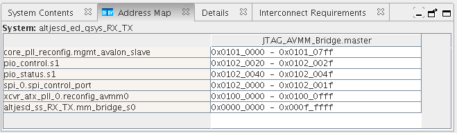
Figure 9. Top Level Platform Designer Address Map