Overview
This tutorial shows you how to use the System Console debugging tool to program a compiled Intel® FPGA design into an Intel® FPGA device, then access the hardware modules (i.e. peripherals) that are instantiated in that Intel FPGA design. This System Console tutorial is based on the Intel FPGA design created in the “Build a Custom Hardware System” tutorial. In that tutorial, you create this Qsys system:
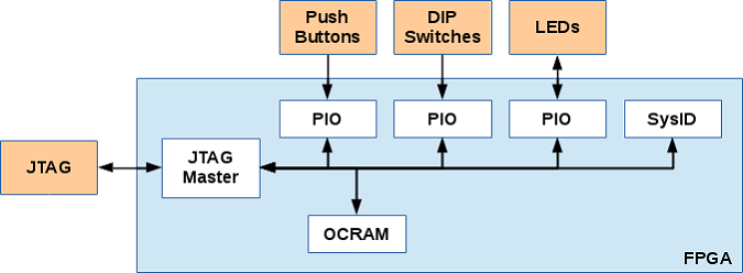
Figure 1. System Block Diagram
In this tutorial, you will interact with the Qsys system through a JTAG cable connected to the Intel FPGA, sending read and write transactions through the JTAG primary component to interact with the secondary peripherals connected to it.
Materials
Hardware
- Windows* or Linux* development host PC
- Terasic DE10-Nano development board and power cable
- USB Type A to Mini-B cable
Software
- Intel® Quartus® Prime Software Suite (either the Lite or Standard Edition, but not the Pro Edition). This was accomplished in the How to Program Your First Intel FPGA tutorial.
- A completed Intel Quartus software project from the Build a Custom Hardware System tutorial. If you have not completed that tutorial you can:
- Click here to complete the Build a Custom Hardware System tutorial.
- Click here to download a zip file which contains the completed project files from the Build a Custom Hardware System tutorial. Unzip the files to a unique project folder on your PC.
Preparing the Board
-
Plug the mini-USB cable into the USB Blaster connector of the board. Then plug the other end of the USB cable to your host PC.
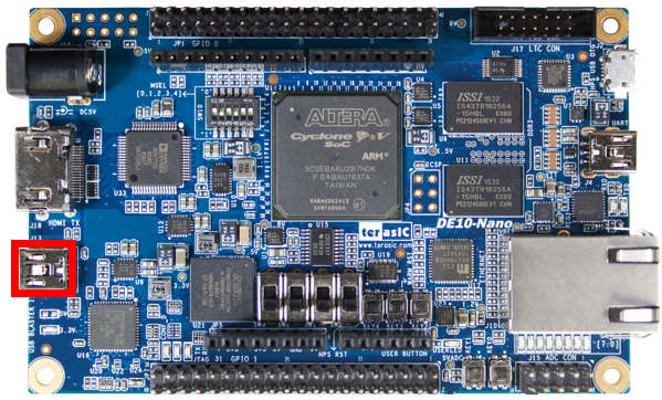
Figure 2. USB Connector -
If the SDCard is installed, please remove it.
Why should I remove the SD Card?
The default behavior of the DE10-Nano kit is to boot from the SD Card. The processor boots, then configures the FPGA under software control. If you leave the SD Card plugged into the board and then reprogram the FPGA, a watchdog timer in the processor would eventually timeout since the FPGA can no longer respond to the processor because the image has changed. The timeout would force a warm reset which would cause the FPGA to be reprogrammed, overwriting the “blink” design you just downloaded.
This behavior is how the DE10-Nano kit was designed to operate by default, but is not the way all systems have to behave. You decide how the system responds to warm and cold reset. You may choose to leave the FPGA running “as is” when a processor reset condition occurs.
- Connect the DC power adapter (5V) to the power outlet. Then plug the other end of the DC power adapter to the development board.
Getting Started with System Console
This section describes how to use System Console to download the Intel FPGA design into the Intel FPGA device, and then interact with the JTAG master IP core inside the Qsys system to read from, and write to the attached slave peripherals. It also demonstrates JTAG link debug and Qsys system health observability provided by System Console.
- Launch the Intel Quartus software and open the blink project you created in the “Build a Custom Hardware System” tutorial by selecting File > Open Project, navigating to your project folder, and selecting the blink.qpf file.
-
Launch System Console from the Tools > System Debugging Tools > System Console menu.
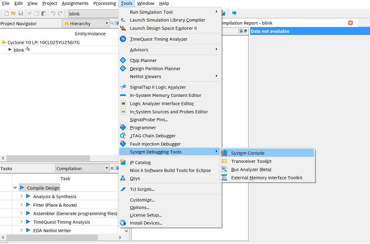
Figure 3. System Console Menu -
The System Console tool looks for devices connected to the JTAG cable. To list the available devices, locate the TCL Console pane at the bottom right corner of the System Console window, and type the following command, then press ENTER:
get_service_paths device
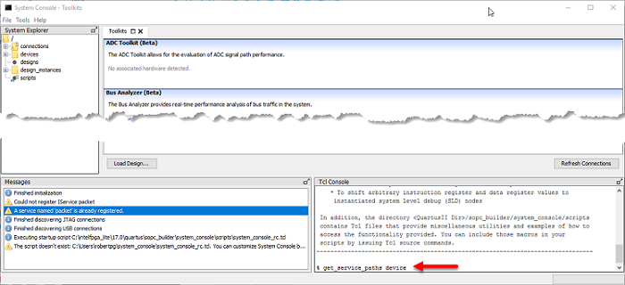
Figure 4. System Console’s TCL Console -
You can use tab completion to finish commands as you type them, and even show you what possible commands can complete from the prefix you type. For instance, type get on the command line and then press TAB, to see a pop-up list of all commands that begin with get. You can use the up and down arrows on the keyboard to scroll up and down the list to select one of the commands. Press Enter to select a command from the pop-up menu.
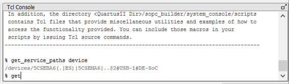
Figure 5. Command Line Before Pressing Tab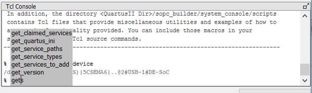
Figure 6. Command Line after Pressing TabThe TCL console history buffer can also be scrolled backward and forward using the up and down arrows on the keyboard, letting you easily recall previously executed command lines.
-
All commands provide help if you pass them into the help command. At the tcl prompt type:
help get_service_paths
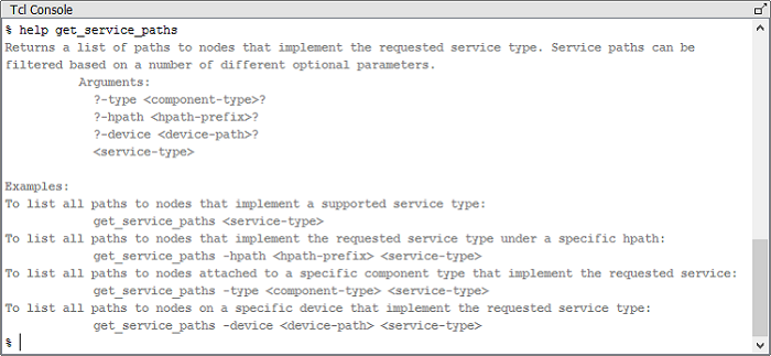
Figure 7. Getting Help for Commands - Type help help to see a list of commands.
Program the Intel® FPGA
-
To program the Intel FPGA device, we first need to get a service path to the device. We will assign that path to a variable called d_path by typing the following command:
set d_path [lindex [get_service_paths device] 0 ]
-
Download the SOF file to the device by typing the following command:
device_download_sof $d_path output_files/blink.sof
The amber D5 CONFIG LED should be illuminated once the commands above complete
Using the JTAG Debug Service
Exercise the JTAG DEBUG service path provided by the JTAG master component.
-
Locate the JTAG DEBUG service path of the JTAG master and store it in a new variable called jd_path by typing the following command:
set jd_path [lindex [get_service_paths jtag_debug] 0]
-
Exercise the JTAG interface by sending a list of values through a loopback at tdi and tdo of a system-level debug node (SLD). This command checks the physical interface of the board and JTAG TAP controller pins of the Intel FPGA device. Type the following command and observe the values returned:
jtag_debug_loop $jd_path [list 1 2 4 8 15 16]
-
Check the clock connected to the JTAG master component in the Qsys system. This command senses whether the clock is active, and returns a 1 if it is, and a 0 if it is not. Type the following command:
jtag_debug_sense_clock $jd_path
-
Sample the “state” of the clock connected to the JTAG master component. Repeatedly sample the clock until you catch it in both the high (1) and low (0) state. Type the following command and press ENTER to observe the clock state. Repeat the command by pressing the up arrow followed by ENTER:
jtag_debug_sample_clock $jd_path
-
Sample the reset signal connected to the JTAG master component inside the Qsys system. The S3 push button on the board is connected to the Qsys system reset input (active low). To sample the reset signal type the following command:
jtag_debug_sample_reset $jd_path
-
To see the reset signal change, press and hold the Key 0 push button and resample the reset, then release the Key 0 push button and resample the reset.
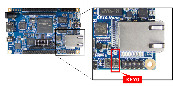
Figure 8. Location of Key 0 Push Button
Using the JTAG Master Service
Next, we will exercise the master service path provided by the JTAG master. This will require us to recall the address map produced in the previous “Build a Custom Hardware System” tutorial. Remember that we used the sopc-create- header-files in that tutorial to create the master_0.h header file, and then dumped the base address macros from that file. To refresh your memory, here is what those addresses are:
# define OCRAM_64K_BASE 0x0
# define LED PIO BASE 0x10000
# define BUTTON PIO BASE 0x10010
# define SWITCH_PIO_BASE 0x10020
# define SYSTEM_ID_BASE 0x10030
-
First, set several TCL variables to allow us to more easily recall these base addresses in the rest of this tutorial. Execute each of the following commands to setup these variables:
set ocram 0x0 set led 0x10000 set button 0x10010 set switch 0x10020 set sysid 0x10030 -
To communicate with the peripherals in the device, we are going to use the “master” service. Locate the service path to the JTAG Master component and save it to the tcl variable m_path by typing the following command:
set m_path [lindex [get_service_paths master] 0 ]
Claim the master service path so that we can interact with the JTAG Master component, and save it to the tcl variable c_path by typing the following command:
set c_path [claim_service master $m_path ""]
Exercise the On-Chip RAM
-
Now that we can send commands to the JTAG Master, let’s interact with the on-chip RAM component by reading a single word from its base address. Type the following command and press ENTER:
master_read_32 $c_path $ocram 1
Now write a word to the base address by typing the following command and pressing ENTER:
master_write_32 $c_path $ocram 0x1234de10
Finally, let’s verify the word was written by reading from the on-chip RAM once more:
master_read_32 $c_path $ocram 1
Exercise the LED PIO
-
Next, we'll use the JTAG Master to interact with the LED PIO component. First, turn on every other LED by typing the following command and pressing ENTER:
master_write_32 $c_path $led 0x55
-
Now turn those LEDs off and turn the other ones on by typing the following command:
master_write_32 $c_path $led 0xaa
-
You can also create a loop to toggle LED0 and LED1 every half second for 10 times by typing the following commands (or cutting and pasting into the Tcl Console):
set COUNT 0 while {$COUNT < 10} { master_write_32 $c_path $led 0x01 after 500 master_write_32 $c_path $led 0x02 after 500 set COUNT [expr $COUNT + 1] } -
Finally, let’s turn on all the user LEDs with the following command:
master_write_32 $c_path $led 0xff
Reset the system
-
Now that we have some LEDs illuminated, lets exercise the JTAG DEBUG service “reset” functionality. We can assert the reset output signal, generated by the JTAG master component, which is connected to the reset input ports of all the peripherals in the system. Type the following command:
jtag_debug_reset_system $jd_path
After executing that command, the LEDs should all turn OFF, returned to their reset state.
- You can trigger the same reset effect by pressing the Key 0 push button like we did before. Turn ON some LEDs again and try pressing Key 0 to prove that as well.
Exercise the button and switch PIOs
-
Interact with the button PIO component by reading the status of the Key 1 Push Button.
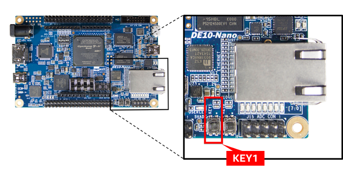
Figure 9. Location of Key 1 Push ButtonFirst, read it before pressing the button with the following command:
master_read_32 $c_path $button 1
-
Interact with the switch PIO component by reading the 4 slide switches, SW1-1 through SW1-4.
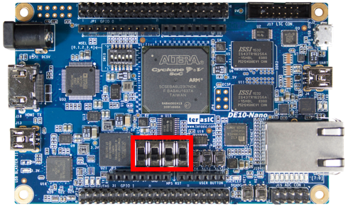
Figure 10. Location of Slide Switches Key 1 Push Button -
First, set SW1-1 through SW1-4 to the OFF position and read the switches with the following command:
master_read_32 $c_path $switch 1
-
Now, one by one, set SW1-4 through SW1-1 to the ON position and read the switches again.
Read the system ID
The System ID peripheral is important since it provides a unique identifier which can be used by software to verify that the executable program was compiled for the actual hardware image configured in the Intel FPGA. If the expected ID stored within the executable does not match the system ID core in the Intel FPGA, it is possible that the software will not execute correctly, and the processor can take the appropriate action (e.g. print a warning message and stop, reconfigure the Intel FPGA, etc.).
-
Read the System ID by typing the following command:
master_read_32 $c_path $sysid 2
The system ID component contains two 32-bit words; the first word is the ID value that we set to 0xde10de10 in the previous hardware portion of this tutorial, and the second word represents the “Unix time” value when the Qsys system was generated.
Using the default slave peripheral
Next, we’ll exercise the default slave peripheral. The default slave peripheral is the place where read/write transactions, to unmapped addresses, are sent. In our system, the default slave is a small RAM.
The peripherals in our system are mapped to addresses 0x0000_0000 thru 0x0001_0038. By reading an address outside that range, we will read instead from the default slave peripheral (which was initialized at device configuration to 0x0000_0000).
-
Read from an unmapped address with the following command:
master_read_32 $c_path 0x01000000 4
The read operation should return the following data:
0x00000000 0x00000000 0x00000000 0x00000000
-
Let’s write 4 words to a different unmapped address.
master_write_32 $c_path 0x02000000 [list 0x0badf00d 0x1badf00d 0x2badf00d 0x3badf00d]
-
Repeat the read operation from another unmapped address and notice that the contents now contain data written in the previous write operation (to an unmapped address):
% master_read_32 $c_path 0x03000000 4 0x0badf00d 0x1badf00d 0x2badf00d 0x3badf00d
-
Now, let’s write to slave that has no write interface, like the system ID peripheral. That write will not be decoded by any slave in the system and will be directed instead to the default slave.
master_write_32 $c_path $sysid 0xfacecafe
-
Verify that this write operation was sent to the default slave by reading from an unmapped address:
master_read_32 $c_path 0x01000000 4 0xfacecafe 0x1badf00d 0x2badf00d 0x3badf00d
The read operation should return the data shown above. Since only a single word was written (0xfacecafe), only the first word of the default slave was changed.
-
Close the master service by typing the following command:
close_service master $c_path
That’s it, you’ve used System Console to debug and test the Intel FPGA hardware system.
As you have seen, System Console is useful for low-level, scripted or interactive testing and debugging of IP cores. In this exercise, we communicated with the device over a JTAG link, but you can also use other communication channels, such as TCP/IP making the tool useful for remote debug as well. For more details on using System Console check out the dedicated web page here.
The next tutorial, My First HPS System, will show you how to instantiate and configure a Hard Processor System (HPS) component using Qsys. Unlike components in the prior "Build a Custom Hardware System" tutorial, the HPS component does not define any soft logic to be configured in the Intel FPGA. Instead, it lets you configure the interfaces of the HPS portion of the Intel® SoC FPGA device. Configuring an entire processor system is a necessarily detailed process, but the level of customization available is an important advantage to using an Intel® SoC FPGA device.