FPGA Transceivers: Connecting the Digital Dots for Faster, Smarter Systems
From unleashing blazing-fast data transmission to powering high-performance applications, discover how FPGA transceiver technology is revolutionizing the world of electronics.
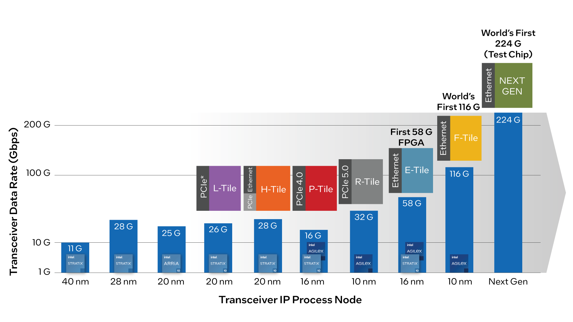
Highest Bandwidth Transceiver Technology1
Transceivers in FPGA devices are essential for high-speed data communication, data serialization/deserialization, protocol adaptation, error handling, and various other tasks in applications that demand high performance, low latency, and flexibility. They enable FPGAs to serve as versatile, high-speed data processing and communication platforms in a wide range of industries.
Our leadership in the transceiver technology helps you do more with your FPGA designs for the most bandwidth-intensive applications.
Learn How Our Transceiver Technology Meets Your FPGA Design Requirements
Design and Debugging Tools
Supports Backplane Application
- 25G to 116G
- All reach supported - VSR, SR, and MR-OIF compliant
- Multi-protocol switching: PON/OTN
Supports Optical Interconnects
- 100G, 200G, 400G @ 106.25 Gbps line rate
- KR to KR4 compliant
- Multi-protocol switching/tuning
Transceiver Technology in Agilex™ FPGAs
Agilex™ 7 FPGA with High Performance 116G Transceivers
Agilex™ 7 FPGA has the industry's first 116Gbps PAM4 multi-channel and multi-protocol transceivers built into the devices.
Product Comparison Table
| F-Series For power and performance-optimized broad-base applications |
I-Series For high-performance processor interfaces and bandwidth-intensive applications |
M-Series For compute-intensive and high-memory-bandwidth applications |
|---|---|---|
| 64 transceiver channels |
Up to 120 transceiver channels | 64 transceiver channels |
| Up to 58Gbps transceivers | Up to 116Gbps transceivers | Up to 116Gbps transceivers |
| PCIe 4.0 x16 | PCIe 5.0 x16 | PCIe 5.0 x16 |
| - | Compute Express Link (CXL) to Intel® Xeon® Scalable processor | Compute Express Link (CXL) to Intel® Xeon® Scalable processor |
| - | - | HBM2e (up to 32 GB) |
Heterogeneous System-in-Package (SiP) Integration
| Transceiver Tile Options | E-Tile | F-Tile | P-Tile | R-Tile | ||
|---|---|---|---|---|---|---|
| Maximum Channel Count and Data Rate | NRZ | PAM4 | NRZ | PAM4 | NRZ | NRZ |
| 24 x 28.9G | 12 x 57.8G | 16 x 32G | 12x 58G and 4 x 116G1 | 16 x 16G | 16 x 32G | |
| Hard IP | 10/25/100GbE | PCIe 4.0 x 16 and 10/25/50/100/200/400GbE |
PCIe 4.0 x 16 | PCIe 5.0 x 16 / CXL v1.1 | ||
| Flexible Protocol Support | Limited | Yes | No | No | ||
Agilex™ 5 FPGA with Transceiver Integration into the FPGA Fabric
Intel's mid-range FPGA series enables high-performance and low-latency FPGA designs due to its integration into the fabric. These FPGAs are perfect for embedded applications requiring small form factor.
Product Comparison Table
| E-Series Optimized for power and size-Ideal for intelligent applications at the edge, embedded, and more |
D-Series Optimized for performance and power efficiency - Ideal for various applications across multiple markets |
|---|---|
| Up to 24 x 28G transceivers | Up to 32 x 28G transceivers |
| Up to PCIe 4.0 x4 and 10/25GbE x6 Hard IP | Up to PCIe 4.0 x8 and 25GbE x16 Hard IP |
| MIPI D-PHY v2.5 at up to 3.5 Gbps per lane | |
Product and Performance Information
Performance varies by use, configuration and other factors. Learn more at www.intel.com/PerformanceIndex. Performance results are based on testing as of dates shown in configurations and may not reflect all publicly available updates. See backup for configuration details. No product or component can be absolutely secure. Your costs and results may vary.