![]()
|
|
|
|
|
|
Example of Moving an Atom in the Chip Planner |
|
You can move logic cells and I/O atoms using the drag and drop method in the Chip Planner. There are two steps in this process: first, you move an atom to a new location in Chip Planner, then you establish routing to the atom at the new location, by running the Check and Save All Netlist Changes command.
The following example illustrates how to move a logic cell atom using the Chip Planner:
Open a compiled design in the Chip Planner.
Select the ECO editing mode.
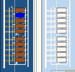
Select the logic cell atom that you want to move.
![]()
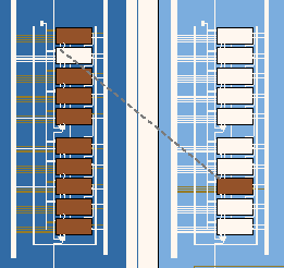
Drag the selected atom to the target location. The Chip Planner moves the atom to the new location and displays a dotted line indicating the move. Its former location is shown as unused.
![]()
If you have the Change Manager open, you can see the move represented as a change in location index.
![]()
Establish routing to the new atom—and verify the validity of the connectivity you have created—by clicking Check and Save All Netlist Changes on the toolbar in either the Chip Planner or the Resource Property Editor.
![]()