![]()
|
|
|
|
|
|
Example of Creating an Atom in the Chip Planner |
|
You can create new logic cell and I/O atoms using the Chip Planner. There are four major steps in this process: first, you pick an unused atom location in the Chip Planner, next you create a new atom at that location, then you create connectivity for the new atom using the Resource Property Editor, and finally, you perform a Check and Save All Netlist Changes command to verify the new atom and establish its routing.
|
|
Note: The following example illustrates the creation of a logic cell atom for a Stratix device; displayed dialog boxes vary slightly for other atom types and devices. |
The following example details the creation of a logic cell atom using the Chip Planner:
Open a compiled project in the Chip Planner.
In the Editing Mode list, select the ECO editing mode.
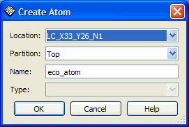
Right-click an unused logic cell atom, and then click Create Atom.
In the Create Atom dialog box, type a name for the new atom.
![]()
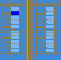
The new atom is now created and drawn in a dark color, indicating that it is being used. The background of the entire LAB also darkens, indicating increased resource usage.
![]()
The Change Manager records the creation of the new atom as a composite action, consisting of the creation of the atom, the addition of signals (if required), and the subsequent assignment of a location index.
![]()
Right-click the new atom in the Chip Planner. The atom turns blue, indicating that it is selected. On the Shortcut menu, click Locate in Resource Property Editor.
Establish connections to the new atom using the connectivity-change tools in the Resource Property Editor.
Establish routing to the new atom—and verify the validity of the connectivity you have created—by clicking Check and Save All Netlist Changes on the toolbar in either the Chip Planner or the Resource Property Editor.
![]()