![]() Executive Summary
Executive Summary
LLT and other time-sensitive applications are ideal use cases for FPGA acceleration. To address this market, Flyslice Technologies developed the FA728Q FPGA-based acceleration card. The FA728Q acceleration platform provides powerful FPGA resources, abundant storage capacity, and easy-to-use interfaces for end users. To expedite, simplify, and standardize the development of their acceleration board, Flyslice Technologies used the OFS infrastructure, which provides a powerful methodology for the rapid development of FPGA solutions using a ‘take and tailor’ approach. Using the OFS infrastructure, Flyslice Technologies integrates its TCP/IP offload engine into the open-source base FIM, commonly called an FPGA ‘shell’.
Background and Challenge
LLT is the modern practice of electronically executing trades of financial securities with minimal time delay between order entry and order execution. Large investment banks, hedge funds, and other financial institutions commonly use this method. In the past, trades were executed manually instead of electronically, and the execution of transactions varied from seconds to minutes. However, with technological advancements in hardware and corresponding software, systems could be programmed to automatically make buy or sell decisions based on certain market signals and movements, reducing trade execution times to milliseconds. With the broader availability of FPGA-based acceleration products in recent years, transaction times have further reduced to microseconds or sub-microseconds.
At the same time, LLT systems increasingly rely on complex trading algorithm models unique to each trading firm’s particular trading strategy for order book interaction. Solutions require general-purpose processors and special-purpose co-processor computing to meet the trading firms’ power and performance requirements, such as in heterogeneous computing. FPGAs are ideal for implementing tailored trading algorithms; however, programming this hardware acceleration device can be time-consuming and difficult to migrate as FPGA families improve and evolve.
Flyslice Technologies, a company headquartered in China, is actively addressing the demand for data center heterogeneous acceleration and high-performance computing, including the LLT segment. They bring FPGA- based hardware accelerator platforms, FPGA acceleration intellectual property (IP) functions, and FPGA-based platform design services to market.
Solution
To meet the low-latency, standardization, and portability requirements of LLT applications, Flyslice Technologies developed their FA728Q acceleration card, which instantiates an integrated TCP/IP offload engine. To do this, Flyslice Technologies modified the provided base FIM in the open-source release of OFS. Because of the composable architecture and ‘take and tailor’ approach, OFS enabled them to simply port their algorithm to the FA728Q acceleration card while leveraging the rest of the provided infrastructure, including the OFS software drivers and libraries, only making minimal modifications.
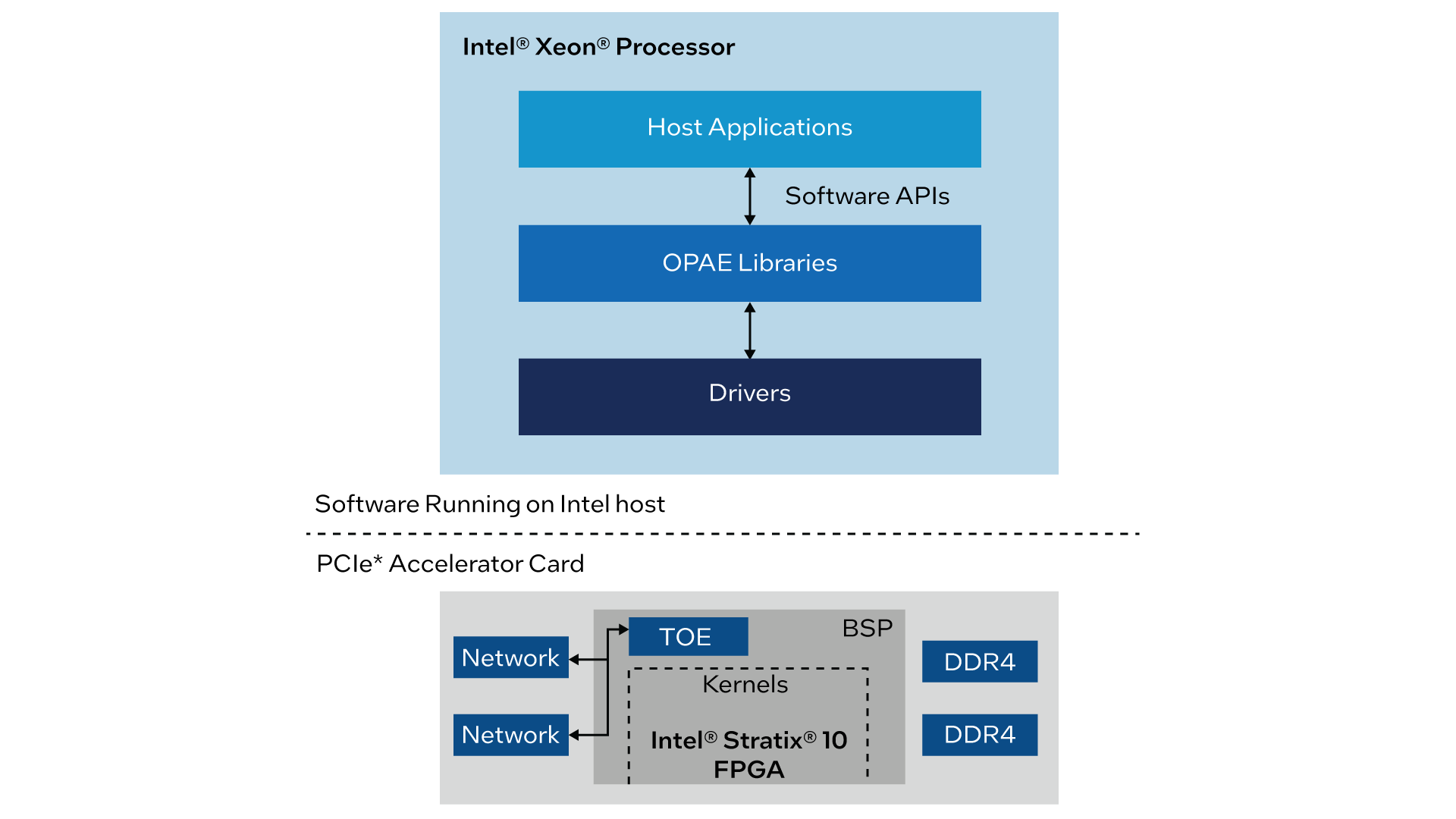
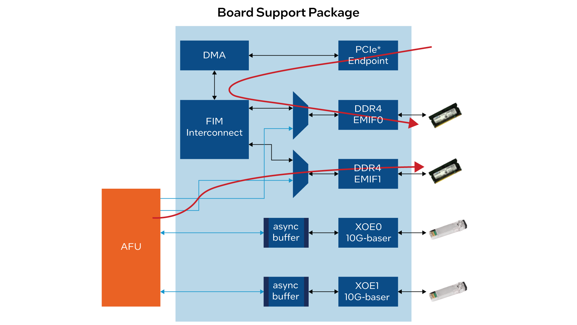
OFS is an open-source hardware and software infrastructure that provides all the key design, software, and infrastructure components needed to jump-start custom FPGA-based board or workload development. The OFS infrastructure consists of the FIM, commonly called a ‘shell,’ and an Accelerator Functional Unit (AFU) region, a designated region for workload development. Using OFS, FPGA board – or FIM – developers can leverage the open-source infrastructure – or base FIM – to quickly develop a tailored, customized FIM for their board based on the target application or industry. OFS also ships with a oneAPI Accelerator Support Package (ASP), which can be leveraged to abstract the FPGA hardware and design flow. OFS saves developers time, increases portability across FPGA generations, uses industry-standard interfaces, and provides an optional high-level design flow using oneAPI.
The FA728Q acceleration card is available today and is a high-end PCIe-based FPGA acceleration board that offers 32 GB onboard DDR4 memory and three QSFP28 sockets to support up to 100 GbE for each interface. The FA728Q acceleration card is also enabled with oneAPI through the OFS infrastructure, so customers can implement their kernels in RTL or migrate algorithms from CPU/GPU to high- level design languages, including C/C++. The Intel oneAPI Base Toolkit also helps synthesize and optimize the kernels to FPGA resources, further improving time to market.
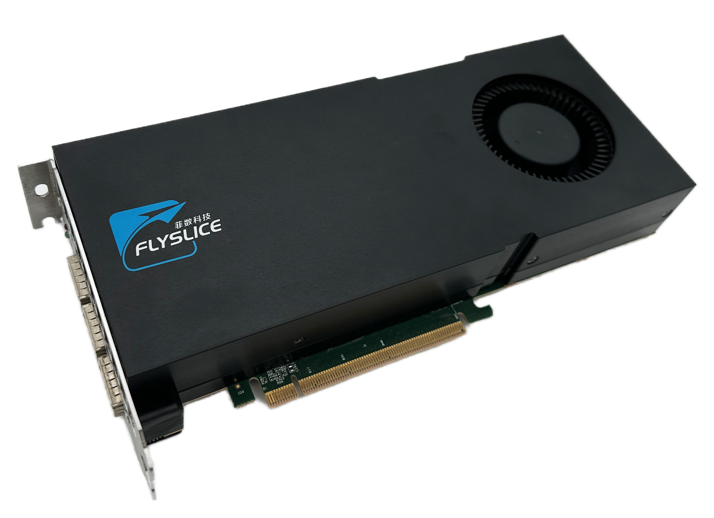
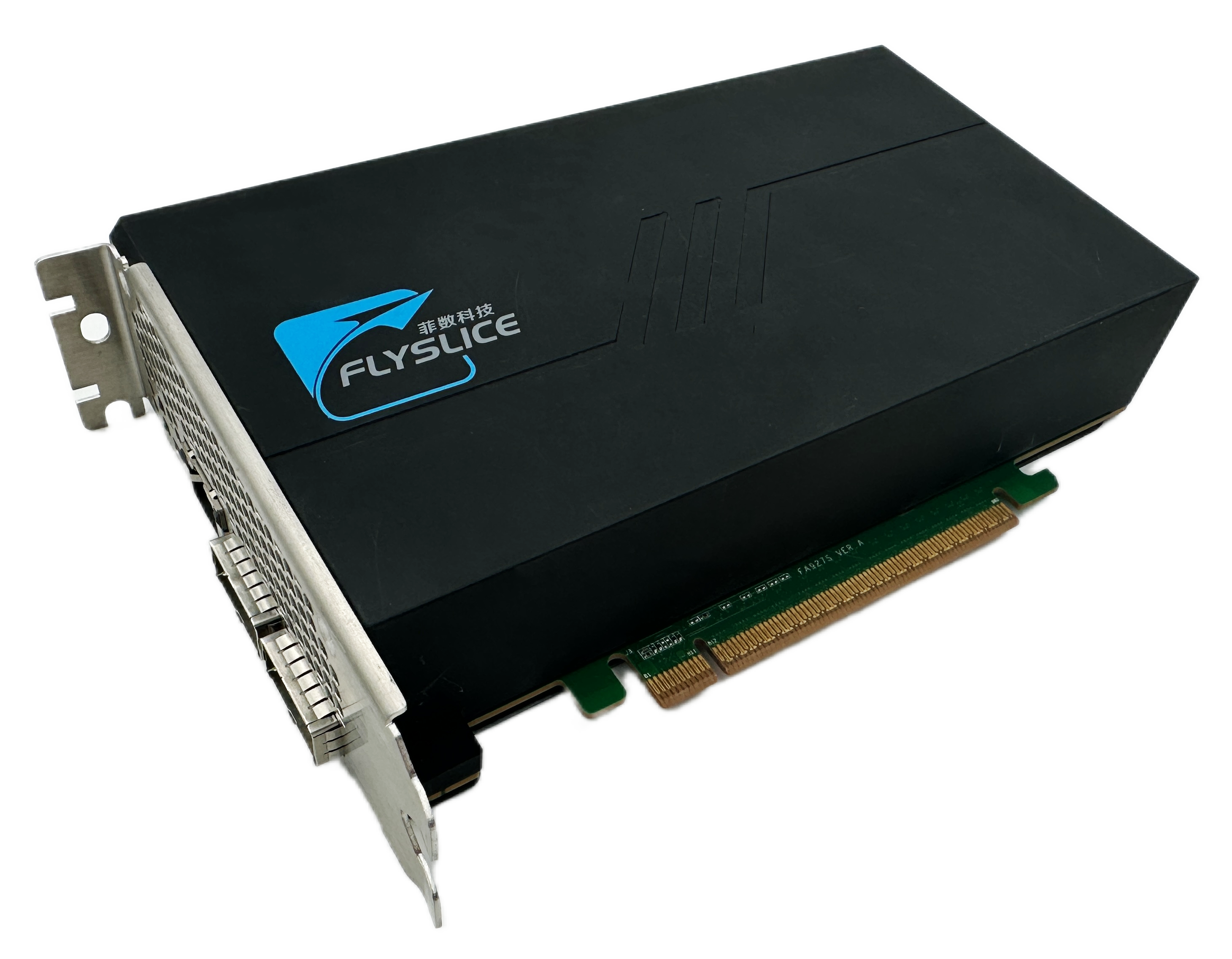
Flyslice Technologies has also begun development on Intel Agilex® FPGA-based boards, including the FA927S card using the Intel Agilex 7 FPGA I-Series and the FA925E card using the Intel Agilex 7 FPGA F-Series.
The FA927S card features high transceiver rates of up to 116 Gbps, PCIe 5.0 x16, and Compute Express Link (CXL) support. It targets bandwidth-intensive applications and is available now for RTL-based development. The FA927S card will support OFS in the first quarter of 2024.
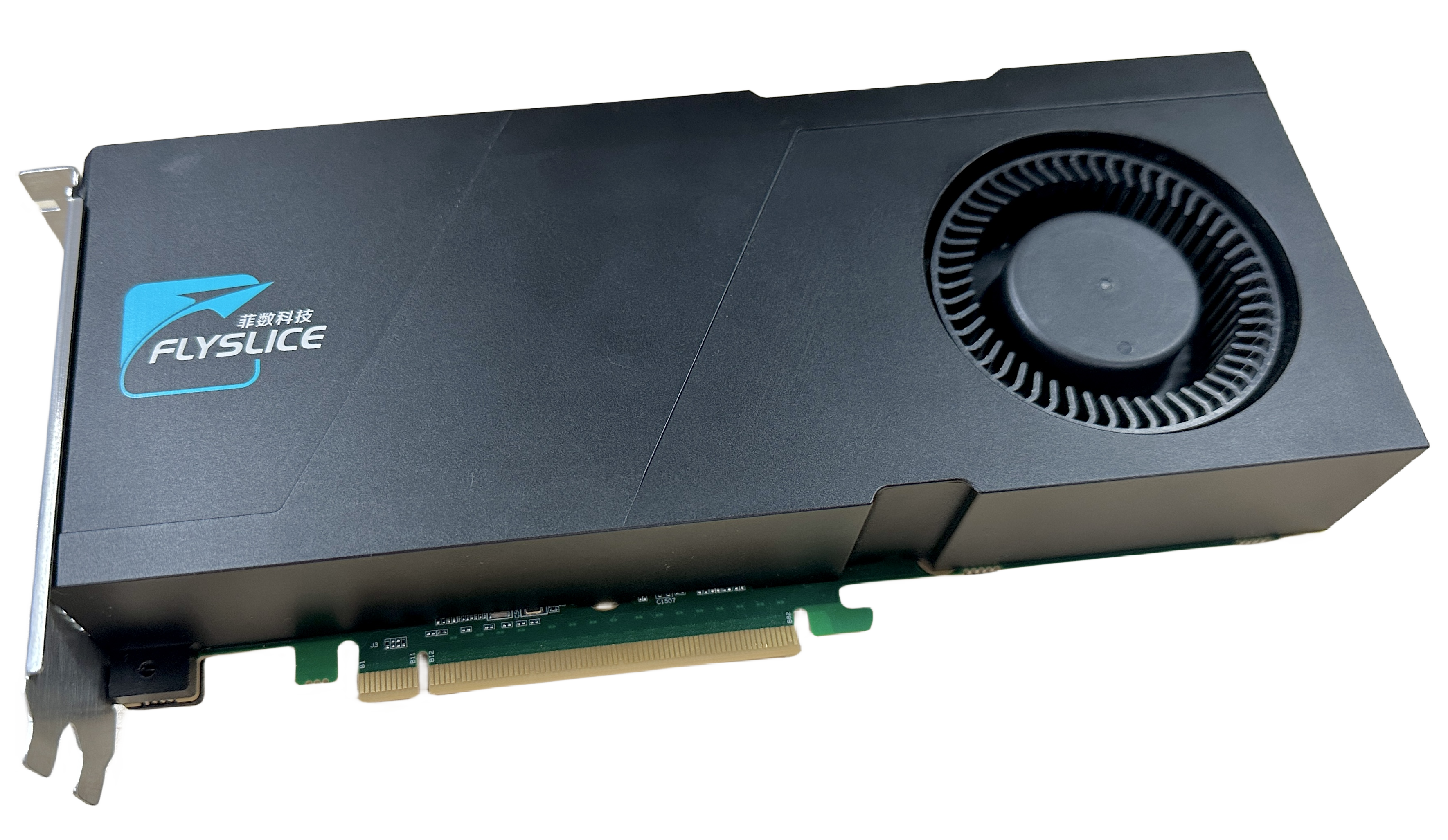
On the other hand, the FA925E card offers four banks of 8 GB and four banks of 4 GB DDR4, totaling 48 GB onboard memory. It is designed for applications with high external memory capacity and bandwidth requirements. The card provides complete support for OFS and will be available by the end of 2023. See Table 1. to compare the three acceleration cards.
Table 1. Comparison Table
|
|
|
|
|
|---|---|---|---|
| Power | 215 W | 200 W | 150 W |
| Cooling Requirement | Active/passive (optional) | Active/passive (optional) | Active/passive (optional) |
| Form Factor | 3/4 length, full-height, dual-slot PCIe | Half-length, full-height, dual-slot PCIe | 3/4 length, full-height, dual-slot PCIe |
| Networking Interfaces | Triple QSFP28 ports: 3 x 100 GbE / 40 GbE | Dual QSFP28 ports: 2 x 100 GbE / 40 GbE | Dual QSFP28 ports 2 x 100 GbE / 40 GbE |
| Memory Interfaces | 4 x 8 GB DDR4, 2,400 MHz with ECC | 4 x 8 GB DDR4, 2,400 MHz with ECC | 4 x 8 GB and 4 x 4 GB DDR4, 2,400 MHz with ECC |
| PCIe Interfaces | - | 5.0 x16 | - |
| Extension Interfaces | - | 2 x8 slim SAS connectors for PCIe 4.0 extension | - |
| Management Port | Micro-USB | Micro-USB | Micro-USB |
| FPGA Device | 1SX280HN2F43E2VG | AGIB027R29A1E2VR3 | AGFB027R25A2E2V |
Results
The offload engine IP function implemented by Flyslice Technologies on the FA728Q card is optimized for latency and performance to meet LLT requirements. In speedup mode, the TCP transmit latency is less than 100 ns, ensuring stable and low-latency connections for time-critical network applications. Table 2. shows the measured latency for various connections. Table 3. shows the high-bandwidth PCIe 3.0 x16 and DDR interfaces.
| Specification | Value |
|---|---|
| Maximum TCP/UDP connections | 63 for TCP, 63 for UDP |
| TCP TX latency (speedup mode) | 15 clocks |
| TCP TX latency (non-speedup mode) | 46 clocks |
| TCP RX latency | 32 clocks |
| UDP TX latency | 42 clocks for a 512-byte packet 18 clocks for 128-byte packet |
| UDP RX latency | 23 clocks |
| Loopback latency for oneAPI kernels | 18 clocks |
Table 2. TCP/IP Offload Engine (TOE) specification
Note:
1. One clock period is 6.4ns
2. TX latency is counted from the falling edge of packet EOP to valid data in XGMII TXC
3. RX latency is counted from packet SOP to valid data in XGMII RXC
| Data Path | Bandwidths |
|---|---|
| Host write memory | 8,287.68 MBps for 8,192-KB block |
| Host read memory | 8,241.19 MBps for 8,192-KB block |
| Kernel write memory | 16,909.6 MBps for 4,096-MB block |
| Kernel read memory | 17,340.3 MBps for 4,096-MB block |
Table 3. Bandwidth provided by each interface
OFS helped us to build a required acceleration platform more easily and quickly for customers, from software APIs drivers to underlying hardware as a full set of equipment.
How to Get Started with FPGA Acceleration Using OFS
FPGA developers can leverage the FA728Q accelerator card and OFS-enabled board, using the open-source documentation and source code to start building their custom workload.
The following table outlines how a developer can start FPGA-based workload development using the Flyslice Technologies acceleration board.
| Leverage FPGA Acceleration for Your Workload | |
|---|---|
| Step 1: Choose a board | View Flyslice Technologies' OFS-enabled board, the FA728Q accelerator card |
| Step 2: Evaluate OFS open-source resources |
Flyslice Technologies will provide the corresponding version of the OFS technical documentation. |
| Step 3: Access open-source hardware and software code |
Flyslice Technologies will provide the corresponding OFS software and hardware code. This is their specific distribution of the OFS base code provided by Intel. |
| Step 4: Develop workload using RTL or C/C++ (using oneAPI) |
Follow the OFS RTL flow OR OFS enables the compulation of oneAPI kernels. Utilize the oneAPI development flow and build FPGA workloads in C/C++. |