External Memory Interfaces (EMIF) IP User Guide: Agilex™ 5 FPGAs and SoCs
- 4.1.2. s0_axi4_clock_out for Agilex 5 E-Series External Memory Interfaces (EMIF) IP - DDR4 Component
- 4.2.2. s0_axi4_clock_out for Agilex 5 E-Series External Memory Interfaces (EMIF) IP - DDR5 Component
7.3.4.1. Address and Command Pin Placement for DDR5
| Address/Command Lane | Index Within Byte Lane | Scheme 1 UDIMM/SODIMM/Component |
Scheme 2 RDIMM |
|---|---|---|---|
| AC1 | 11 | CK_C[1] | SCL 1 (i3c) |
| 10 | CK_T[1] | SDA 1 (i3c) | |
| 9 | CS_N[0] | CS_N[0] | |
| 8 | CS_N[1] | CS_N[1] | |
| 7 | CK_C[0] | CK_C[0] 1 | |
| 6 | CK_T[0] | CK_T[0] 1 | |
| 5 | CA[12] | ||
| 4 | CA[11] | ||
| 3 | RESET_N | RESET_N 1 | |
| 2 | RZQ Site | ||
| 1 | ALERT_N | ALERT_N | |
| 0 | CA[10] | ||
| AC0 | 11 | Differential "N-Side" reference clock input site | |
| 10 | Differential "P-Side" reference clock input site | ||
| 9 | CA[9] | LBD, RSP_A_n 1 | |
| 8 | CA[8] | LBS, RSP_B_n 2 | |
| 7 | CA[7] | PAR_A | |
| 6 | CA[6] | CA[6] | |
| 5 | CA[5] | CA[5] | |
| 4 | CA[4] | CA[4] | |
| 3 | CA[3] | CA[3] | |
| 2 | CA[2] | CA[2] | |
| 1 | CA[1] | CA[1] | |
| 0 | CA[0] | CA[0] | |
|
Note:
|
|||
The Agilex™ 5 EMIF IP for DDR5 supports fixed Address and Command pin placement as shown in the above table. The IP supports up to 2 ranks for the following schemes:
- Scheme 1 supports component, UDIMM, and SODIMM.
- Scheme 2 supports RDIMM.
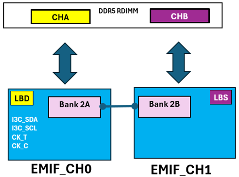
The above figure shows only I3C_SDA, I3C_SCL, CK_T, CK_C, LBD and LBS. To implement one DDR5 RDIMM (2 channel) interface, two adjacent IO 96B banks on the same side of the device are required.
Connect EMIF_CH0 signals to CHA on the RDIMM, and the signals for EMIF_CH1 to CHB on the RDIMM respectively.
You cannot swap the pin location for LBD with LBS. Place LBD on the I/O bank where EMIF_CH0 resides and connect LBD to pin number 86 on the DIMM connector. Place LBS on the I/O bank where EMIF_CH1 resides and connect LBS to pin number 87 on the DIMM connector.