Agilex™ 7 F-Series and I-Series FPGA Memory Subsystem IP User Guide
ID
789389
Date
7/15/2024
Public
1. About the Agilex™ 7 F-Series and I-Series FPGA Memory Subsystem IP
2. Introduction to Memory Subsystem IP
3. Memory Subsystem IP Architecture and Feature Description
4. Memory Subsystem Features
5. Memory Subsystem Interfaces and Signals
6. Memory Subsystem User Operations
7. Memory Subsystem Register Descriptions
8. Parameterizing the Memory Subsystem IP
9. Simulating a Design Example
10. Document Revision History for Agilex™ 7 F-Series and I-Series FPGA Memory Subsystem IP User Guide
5.3.1. TCAM AXI-ST Request Interface
5.3.2. TCAM AXI-ST Response Interface
5.3.3. TCAM AXI-Lite Interface
5.3.4. BCAM AXI-ST Request Interface
5.3.5. BCAM AXI-ST Response Interface
5.3.6. BCAM AXI-Lite Interface
5.3.7. MBL AXI-ST Request Interface
5.3.8. MBL AXI-ST Response Interface
5.3.9. MBL AXI-Lite Interface
6.4.1. MBL Flush Operation
6.4.2. MBL Insert Key Operation
6.4.3. MBL Delete Key Operation
6.4.4. MBL Lookup Operation Using Key
6.4.5. MBL Modify Operation
6.4.6. MBL Modify Result Using Handle Operation
6.4.7. MBL Delete Key Using Handle Operation
6.4.8. MBL Lookup Using Handle Operation
6.4.9. MBL Insert Key if Not Present or Modify Result if Present Operation
6.4.10. MBL Get Handle Operation
7.2.1. Offset 0x0000 Version
7.2.2. Offset 0x0004 Feature List
7.2.3. Offset 0x0010 Memory Interfaces 0-7
7.2.4. Offset 0x0014 Memory Interfaces 8-15
7.2.5. Offset 0x0018 Memory Interfaces 16-23
7.2.6. Offset 0x001C Memory Interfaces 24-31
7.2.7. Offset 0x0020 Scratch Pad
7.2.8. Offset 0x0030 Control Policy (Lower DWORD)
7.2.9. Offset 0x0034 Control Policy (Upper DWORD)
7.2.10. Offset 0x0038 Read Access Control Policy (Lower DWORD)
7.2.11. Offset 0x003C Read Access Control Policy (Upper DWORD)
7.2.12. Offset 0x0040 Write Access Control Policy (Lower DWORD)
7.2.13. Offset 0x0044 Write Access Control Policy (Upper DWORD)
7.2.14. Offset 0x0050 Memory Status Bitmask 0
7.2.15. Offset 0x0054 Memory Status Bitmask 1
7.2.16. Offset 0x0058 Memory Ready Status 0
7.2.17. Offset 0x005C Memory Ready Status 1
7.2.18. Offset 0x0060 Memory Error Status 0
7.2.19. Offset 0x0064 Memory Error Status 1
7.3.2.1. Version
7.3.2.2. Feature List
7.3.2.3. Interface Attribute Parameters
7.3.2.4. Interface Attribute Parameters 1
7.3.2.5. Scratch Pad
7.3.2.6. General Control (GEN_CTRL)
7.3.2.7. Management Control (MGMT_CTRL)
7.3.2.8. Hash function_0 seed
7.3.2.9. Hash function_1 seed
7.3.2.10. Hash function_2 seed
7.3.2.11. Warning 0 (WARNING_0)
7.3.2.12. Fatal Error (FATAL_ERROR_0)
7.3.2.13. Monitor 0 (MON_)
7.3.2.14. Total Entries (TOTAL_ENTRIES)
7.3.2.15. Max. Rehouse Iterations (Max_Rehouse_Iterations)
7.3.2.16. Statistics Control (STATS_CTRL)
7.3.2.17. Active Table Entries (TABLE_ENTRIES)
7.3.2.18. Key_N
7.3.2.19. Result_N
7.5.1. MBL DFH
7.5.2. General MBL Registers
7.5.3. Version
7.5.4. Mbl_scratch
7.5.5. Mbl_gen_ctrl
7.5.6. Mbl_mgmt_ctrl
7.5.7. Mbl_key_handle
7.5.8. Mbl_nxt_handle_req
7.5.9. Mbl_nxt_handle
7.5.10. Mbl_warning_0
7.5.11. Mbl_fatal_0
7.5.12. Mbl_mon_0
7.5.13. Mbl_total_entries
7.5.14. Mbl_total_rehashes
7.5.15. Mbl_max_used_bins
7.5.16. Mbl_stats_ctrl
7.5.17. Mbl_stats_result
7.5.18. Mbl_max_lkup_latency
7.5.19. Mbl_max_rehash_index
7.5.20. Mbl_key
7.5.21. Mbl_res
8.2.5.1. Parameterizing the External Memory Interface (EMIF) IP
8.2.5.2. Parameterizing the Memory-Specific Adapter
8.2.5.3. Parameterizing the Content-Addressable Memory (CAM) IP
8.2.5.4. Parameterizing the External Memory Interfaces Calibration IP
8.2.5.5. Saving the IPs Within the Memory Subsystem
8.2.5.6. Propagation of Changes Across IPs within the Memory Subsystem IP
2. Introduction to Memory Subsystem IP
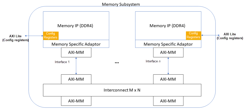
The memory subsystem IP is a high-level solution on top of the External Memory Interfaces Agilex™ 7 FPGA IP, providing an easy way to instantiate up to 8 external memory interfaces (EMIFs) with application-level optimizations.
Depending on your requirements, the memory subsystem provides scalable and composable options that you can use to create effective turn-key solutions. You can easily instantiate the memory subsystem IP through the Quartus® Prime software, which also provides external memory toolkits that you can use to test your implementation of the IP in the FPGA.
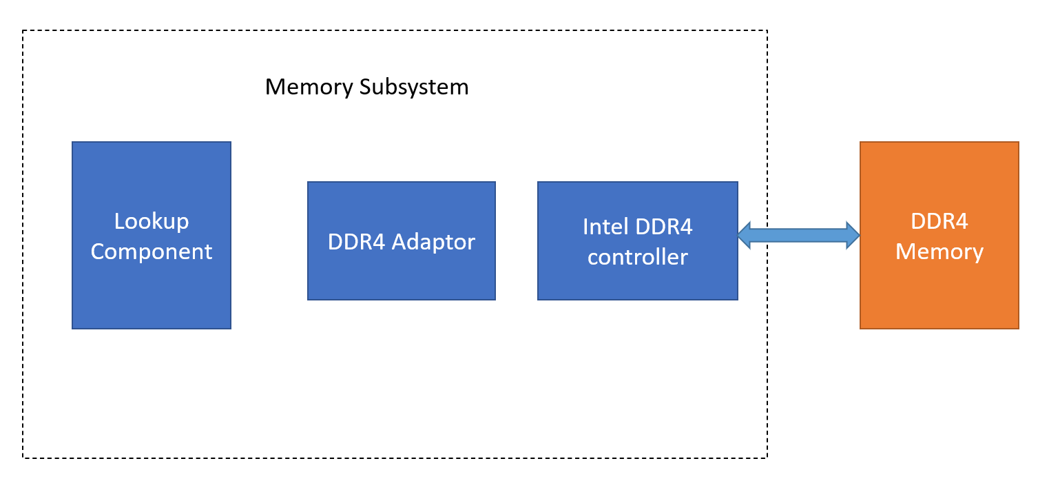
The memory subsystem IP provides the following components:
- Up to 8 lookup IP instances.
- Up to 8 EMIF instances.
- A memory controller that implements all the memory commands and protocol-level requirements.
- A soft logic adapter to boost memory throughput by traffic shaping.
Figure 1. Altera® FPGA IP Memory Subsystem Block Diagram
You can configure the memory subsystem IP for use in various applications such as full crossbar for machine learning, multi-hierarchy memory bridge, or as a memory-specific adaptor with lookup core logic. All the available modes offer common scalability and compose-ability.
Figure 2. Memory Subsystem IP Used as Memory Adaptor with Lookup and One EMIF