A newer version of this document is available. Customers should click here to go to the newest version.
1. FPGA AI Suite SoC Design Example User Guide
2. About the SoC Design Example
3. FPGA AI Suite SoC Design Example Quick Start Tutorial
4. FPGA AI Suite SoC Design Example Run Process
5. FPGA AI Suite SoC Design Example Build Process
6. FPGA AI Suite SoC Design Example Quartus® Prime System Architecture
7. FPGA AI Suite Soc Design Example Software Components
8. Streaming-to-Memory (S2M) Streaming Demonstration
A. FPGA AI Suite SoC Design Example User Guide Archives
B. FPGA AI Suite SoC Design Example User Guide Document Revision History
3.1. Initial Setup
3.2. Initializing a Work Directory
3.3. (Optional) Create an SD Card Image (.wic)
3.4. Writing the SD Card Image (.wic) to an SD Card
3.5. Preparing SoC FPGA Development Kits for the FPGA AI Suite SoC Design Example
3.6. Adding Compiled Graphs (AOT files) to the SD Card
3.7. Verifying FPGA Device Drivers
3.8. Running the Demonstration Applications
7.1.1. Yocto Recipe: recipes-core/images/coredla-image.bb
7.1.2. Yocto Recipe: recipes-bsp/u-boot/u-boot-socfpga_%.bbappend
7.1.3. Yocto Recipe: recipes-drivers/msgdma-userio/msgdma-userio.bb
7.1.4. Yocto Recipe: recipes-drivers/uio-devices/uio-devices.bb
7.1.5. Yocto Recipe: recipes-kernel/linux/linux-socfpga-lts_5.15.bbappend
7.1.6. Yocto Recipe: wic
3.5.1.1. Confirming Agilex™ 7 FPGA I-Series Transceiver-SoC Development Kit Board Set Up
Confirm the board settings as follows:
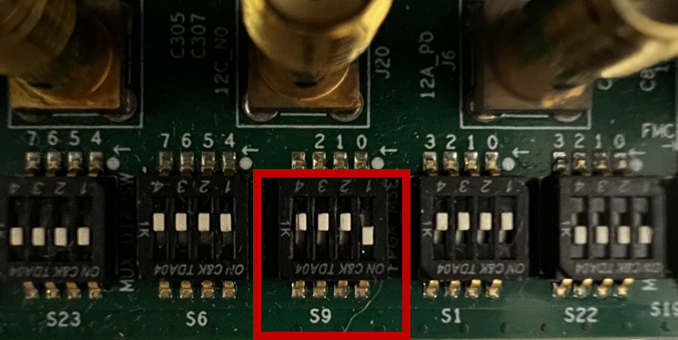
- Ensure that the Agilex™ 7 FPGA I-Series Transceiver-SoC Development Kit has the required DIP switch and jumper settings. The SoC example design requires that all DIP switches have their default settings except for S9 where switch 1 is ON and switches 2,3, and 4 are OFF:
For more details about default DIP switch and jumper settings, refer to Agilex™ 7 FPGA I-Series Transceiver-SoC Development Kit User Guide .
- Ensure that the HPS IO48 OOBE daughter card is installed in connector J4 on the development kit, and the SD card with the programmed Yocto image is installed in the daughter card.
- Ensure that the DDR4 x8 RDIMM is installed in the PCIe slot furthest from the fan. For RDIMM requirements, refer to Agilex 7 FPGA I-Series Transceiver-SoC Development Kit Hardware Requirements.
When configured and connected, the Agilex™ 7 FPGA I-Series Transceiver-SoC Development Kit should resemble the following image:
The board connections serve the following purposes:
-
The USB 2.0 connector is used to program the FPGA device.
-
The Ethernet connector is used for fast data transfer to the HPS.
-
The micro USB connector is used to monitor the serial output from, and provide command-line input to the HPS during operation.