1.2. Generating the Design Example
Figure 3. Procedure to Generate Design Example
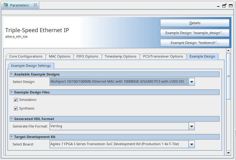
Figure 4. Example Design Tab in the Triple-Speed Ethernet IP Parameter Editor
Follow these steps to generate the hardware design example and testbench:
- In the Quartus® Prime Pro Edition software, click to create a new Quartus Prime project, or to open an existing Quartus Prime project. The wizard prompts you to specify a device.
- Select Agilex™ 7 device family and select a device that has LVDS.
- Click Finish to close the wizard.
- In the IP Catalog, locate and select . The New IP Variation window appears.
- Specify a top-level name <your_ip> for your custom IP variation. The parameter editor saves the IP variation settings in a file named <your_ip>.ip.
- Click OK. The parameter editors appears.
- To generate a design example, select a Multi channel Triple Speed Ethernet MAC PCS Example Design (Agilex) preset from the Presets library and click Apply. When you select a design, the system automatically populates the IP parameters for the design. The parameter editor automatically sets the parameters required to generate the design example. Do not change the preset parameters in the IP tab.
- For Example Design Files, select the Simulation option to generate the testbench, or the Synthesis option to generate the hardware design example.
Note: You must select at least one of the options to generate the design example.
- On the Example Design tab, under Generated HDL Format, select Verilog HDL or VHDL.
Note: If you select VHDL, you must simulate the testbench with a mixed language simulator. The device under test is a VHDL model, but the main testbench file is a System Verilog file.
- Under Target Development Kit, select the Agilex 7 FPGA I-Series Transceiver-SoC Development Kit (Production 1 4x F-Tile) or select None.
Note:
- If you select a specific development kit as the Target Development Kit, the design example is generated based on the specific device and overwrites the device you selected in your project file.
- If you select None as the Target Development Kit, ensure that the selected device is your targeted device and adjust the pins assignment in the .qsf file. By default, the .qsf file is generated based on the device used in the development kit.
- Click the Example Design: “example_design” button. The Select Example Design Directory window appears.
- If you want to modify the design example directory path or name from the defaults displayed (eth_tse_0_example_design), browse to the new path and type the new design example directory name (<design_example_dir>).
Note: You must perform the parameter settings based on the steps above to generate the design example.
- Click OK.