R-Tile Avalon® Streaming FPGA IP for PCI Express* User Guide
4.3.1.1. TLP Header and Data Alignment for the Avalon® streaming RX and TX Interfaces
The TLP prefix, header and data are sent and received on the Avalon® streaming TX and RX interfaces. There are four Avalon® streaming TX/RX interfaces corresponding to the four PCIe cores. The signal names on these interfaces are prefixed with "p0" for the x16 core, "p1" for the x8 core, "p2" for the x4_0 core and "p3" for the x4_1 core.
Each of these interfaces can contain up to four segments. The signal names for these segments are notated with *_st0_*, *_st1_*, *_st2_* and *_st3_*.
A Start of Packet (SOP) symbol demarcates the start of a packet. A TLP with or without data is terminated by an End of Packet (EOP) symbol. An EOP happening on the st0, st1, st2 or st3 segment implies that the last data with data valid = 1 is located on the corresponding data bus.
A TLP without data is qualified by a header valid indicator. A TLP with data is qualified by a data valid indicator. There is also a prefix valid indicator to qualify a TLP Prefix.
If a global valid signal is required for backward compatibility to P-tile, the header valid ORed with data valid will provide the global valid indicator.
This is defined to enable pipelined Header/Prefix and Data transfers to meet the bandwidth target. For example, while transferring the Data for one TLP, the Header and Prefix for the next TLP can also be transferred.
The Avalon® streaming Header and TLP Prefix bus packet format follows the TLP packet format as defined by the PCIe specification for Memory, Configuration and Message TLPs. Refer to TLP Prefix, Header and Data when PCIe Header Format Checkbox is Disabled and TLP Prefix, Header and Data when PCIe Header Format Checkbox is Enabled below for more details.
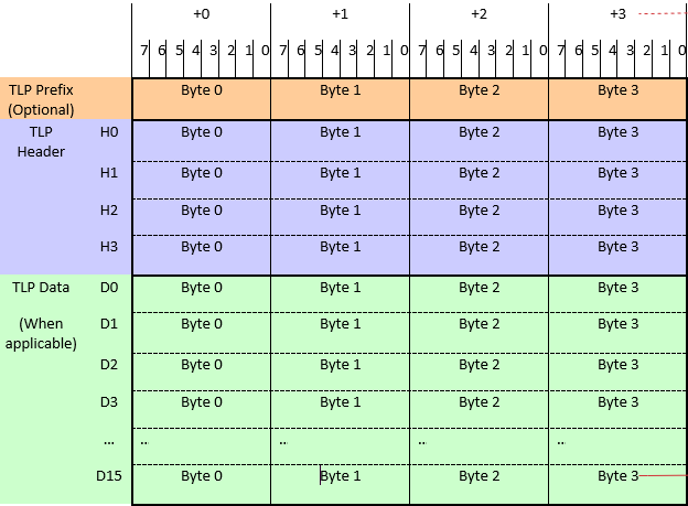
In the R-Tile Parameter Editor, there is a checkbox labeled PCIe Header format (in the PCIe Avalon® Settings tab) that allows you to specify whether the Header will follow the Big Endian format or Little Endian format. If this checkbox is not enabled, the Header follows the Little Endian format as shown in TLP Prefix, Header and Data when PCIe Header Format Checkbox is Disabled (note that the diagram shows the Prefix, Header and Data for one segment of the Avalon® streaming interface, not the whole interface):
If the PCIe Header format checkbox is enabled, the Header follows the Big Endian format as shown in TLP Prefix, Header and Data when PCIe Header Format Checkbox is Enabled:
| Configuration | Link Rate | Width Mode | Header | Data | Application Clock Frequency (MHz) |
|---|---|---|---|---|---|
| 1x16 | Gen5 | Double-Width | st3_hdr[127:0] st2_hdr[127:0] st1_hdr[127:0] st0_hdr[127:0] |
st3_data[255:0] st2_data[255:0] st1_data[255:0] st0_data[255:0] |
400 MHz 425 MHz 450 MHz 475 MHz 500 MHz |
| Gen4 | Double-Width | st3_hdr[127:0] st2_hdr[127:0] st1_hdr[127:0] st0_hdr[127:0] |
st3_data[255:0] st2_data[255:0] st1_data[255:0] st0_data[255:0] |
250 MHz 275 MHz 300 MHz |
|
| Single-Width 7 | st1_hdr[127:0] st0_hdr[127:0] |
st1_data[255:0] st0_data[255:0] |
400 MHz 425 MHz 450 MHz 475 MHz 500 MHz |
||
| Gen3 | Double-Width | st3_hdr[127:0] st2_hdr[127:0] st1_hdr[127:0] st0_hdr[127:0] |
st3_data[255:0] st2_data[255:0] st1_data[255:0] st0_data[255:0] |
250 MHz 275 MHz 300 MHz |
|
| Single-Width 7 | st1_hdr[127:0] st0_hdr[127:0] |
st1_data[255:0] st0_data[255:0] |
400 MHz 425 MHz 450 MHz 475 MHz 500 MHz |
||
| 2x8 | Gen5 | Double-Width | st1_hdr[127:0] st0_hdr[127:0] |
st1_data[255:0] st0_data[255:0] |
400 MHz 425 MHz 450 MHz 475 MHz 500 MHz |
| Gen4 | Double-Width | st1_hdr[127:0] st0_hdr[127:0] |
st1_data[255:0] st0_data[255:0] |
250 MHz 275 MHz 300 MHz |
|
| Single-Width 7 | st0_hdr[127:0] | st0_data[255:0] | 400 MHz 425 MHz 450 MHz 475 MHz 500 MHz |
||
| Gen3 | Double-Width | st1_hdr[127:0] st0_hdr[127:0] |
st1_data[255:0] st0_data[255:0] |
250 MHz 275 MHz 300 MHz |
|
| Single-Width 7 | st0_hdr[127:0] | st0_data[255:0] | 250 MHz 275 MHz 300 MHz |
||
| 4x4 | Gen5 | Double-width | st1_hdr[127:0] st0_hdr[127:0] |
st1_data[127:0] st0_data[127:0] |
400 MHz 425 MHz 450 MHz 475 MHz 500 MHz |
| Gen4 | Double-width | st1_hdr[127:0] st0_hdr[127:0] |
st1_data[127:0] st0_data[127:0] |
250 MHz 275 MHz 300 MHz |
|
| Single-Width 7 | st0_hdr[127:0] | st0_data[127:0] | 400 MHz 425 MHz 450 MHz 475 MHz 500 MHz |
||
| Gen3 | Double-width | st1_hdr[127:0] st0_hdr[127:0] |
st1_data[127:0] st0_data[127:0] |
250 MHz 275 MHz 300 MHz |
|
| Single-Width 7 | st0_hdr[127:0] | st0_data[127:0] | 250 MHz 275 MHz 300 MHz |
- Refer to Section 4.3.1.3.1 and Section 4.3.1.4.1 for Application logic guidelines for the proper handling of the Avalon Streaming interface.