F-Tile Avalon® Streaming Intel® FPGA IP for PCI Express* Design Example User Guide
ID
683372
Date
11/03/2023
Public
A newer version of this document is available. Customers should click here to go to the newest version.
3.3.1.1. Steps to Run Simulation : VCS*
3.3.1.2. Steps to Run Simulation : VCS* MX
3.3.1.3. Steps to Run Simulation : QuestaSim* / ModelSim* - Intel® FPGA Starter Edition / Questa* Intel® FPGA Starter Edition
3.3.1.4. Steps to Run Simulation : Xcelium*
3.3.1.5. Steps to Run Simulation : Riviera-PRO*
3.3.2.2. PIO Design Example Testbench
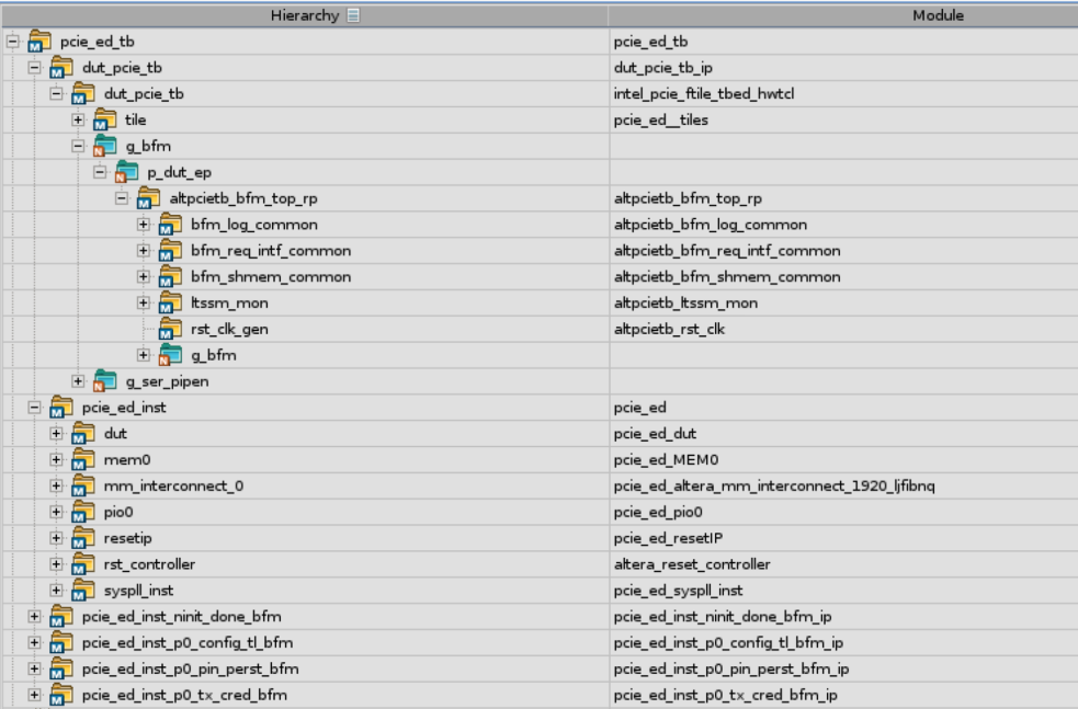
The figure below shows the PIO design example simulation design hierarchy. The tests for the PIO design example are defined with the apps_type_hwtcl parameter set to 3. The tests run under this parameter value are defined in ebfm_cfg_rp_ep_rootport, find_mem_bar and downstream_loop.
Figure 22. PIO Design Example Simulation Design Hierarchy
The testbench starts with link training and then accesses the configuration space of the IP for enumeration. A task called downstream_loop (defined in the Root Port PCIe BFM altpcietb_bfm_rp_gen4_x16.sv) then performs the PCIe link test. This test consists of the following steps:
- Issue a memory write command to write a single dword of data into the on-chip memory behind the Endpoint.
- Issue a memory read command to read back data from the on-chip memory.
- Compare the read data with the write data. If they match, the test counts this as a Pass.
- Repeat Steps 1, 2 and 3 for 10 iterations.
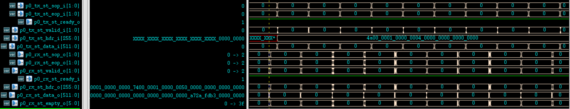
The first memory write takes place around 236 µs. It is followed by a memory read at the Avalon® -ST RX interface of the F-tile Hard IP for PCIe. The Completion TLP appears shortly after the memory read request at the Avalon® -ST TX interface. The memory write and read transactions and the Completion TLP are shown in the following waveforms.
Figure 23. Simulation Waveforms for the PIO Design Example for the F-Tile Avalon® -ST IP for PCIe