25G Ethernet Stratix® 10 Intel® FPGA IP Design Example User Guide
                    
                        ID
                        683252


                    Date
                    6/20/2024
                
                
                    Public


                        1. 25G Ethernet Intel® FPGA IP Quick Start Guide


                        2. 10G/25G Ethernet Single-Channel Design Example for Stratix® 10 Devices


                        3. 25G Ethernet Single-Channel Design Example for Stratix® 10 Devices


                        4. 25G Ethernet Multi-Channel Design Example for Intel Stratix 10 Devices


                        5. 25G Ethernet Intel® FPGA IP Design Example References


                        6. 25G Ethernet Stratix® 10 Intel® FPGA IP Design Example User Guide Archives


                        7. Document Revision History for the 25G Ethernet Stratix® 10 Intel® FPGA IP Design Example User Guide


                                1.1. Directory Structure


                                1.2. Generating the Design Example


                                1.3. Simulating the 25G Ethernet Intel® FPGA IP Design Example Testbench


                                1.4. Compiling and Configuring the Design Example in Hardware


                                1.5. Changing Target Device in Hardware Design Example


                                1.6. Testing the 25G Ethernet Intel® FPGA IP Design in Hardware


                4.4.3. Test Case
The simulation test case performs the following steps:
- Instantiates 25G Ethernet Intel® FPGA IP and ATX PLL.
- Waits for PHY status signal to settle.
- Prints PHY status.
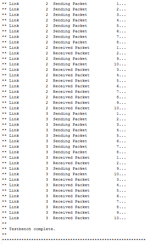
- Analyzes the results. The successful testbench sends and receives packets, and displays "Testbench complete."
   Figure 23. Sample Simulation Output when Ethernet Channel is Configured to 1This figure shows a successful simulation test run when the Ethernet channel (i.e., LINK) is configured to 1.


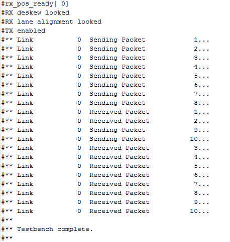
   Figure 24. Sample Simulation Output when Ethernet Channel is Configured to 4 (Part 1 of 2)This figure shows a successful simulation test run when the Ethernet channel (i.e., LINK) is configured to 4.


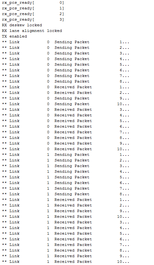
   Figure 25. Sample Simulation Output when Ethernet Channel is Configured to 4 (Part 2 of 2)This figure shows a successful simulation test run when the Ethernet channel (i.e., LINK) is configured to 4.


 