25G Ethernet Stratix® 10 Intel® FPGA IP Design Example User Guide
ID
683252
Date
6/20/2024
Public
1. 25G Ethernet Intel® FPGA IP Quick Start Guide
2. 10G/25G Ethernet Single-Channel Design Example for Stratix® 10 Devices
3. 25G Ethernet Single-Channel Design Example for Stratix® 10 Devices
4. 25G Ethernet Multi-Channel Design Example for Intel Stratix 10 Devices
5. 25G Ethernet Intel® FPGA IP Design Example References
6. 25G Ethernet Stratix® 10 Intel® FPGA IP Design Example User Guide Archives
7. Document Revision History for the 25G Ethernet Stratix® 10 Intel® FPGA IP Design Example User Guide
1.1. Directory Structure
1.2. Generating the Design Example
1.3. Simulating the 25G Ethernet Intel® FPGA IP Design Example Testbench
1.4. Compiling and Configuring the Design Example in Hardware
1.5. Changing Target Device in Hardware Design Example
1.6. Testing the 25G Ethernet Intel® FPGA IP Design in Hardware
3.4.4. Test Case—Design Example with the IEEE 1588v2 Feature
Note: For 25G Ethernet single-channel design example with IEEE 1588v2 feature simulation testbench, refer to Functional Description.
The simulation test case performs the following actions:
- Instantiates , ATX PLL, and IO PLL (sampling PLL).
- Waits for RX clock and PHY status signal to settle.
- Prints PHY status.
- Checks for 10 valid data.
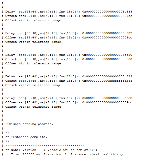
- Analyzes the results. The successful testbench displays "Testbench complete." when the PTP delay and offset data are within the threshold values.
The following sample output illustrates a successful simulation test run:
#
# Waiting for RX alignment...
# iatpg_pipeline_global_en is set
# iatpg_pipeline_global_en is set
# RX deskew locked.
# RX lane aligmnent locked.
#
# Sending packets...
#
# Delay (sec[95:48],ns[47:16],fns[15:0]): 0x000000000000000000064457
# Offset(sec[95:48],ns[47:16],fns[15:0]): 0x000000000000000000000000
# Offset within tolerence range.
#
#
# Delay (sec[95:48],ns[47:16],fns[15:0]): 0x000000000000000000064bb4
# Offset(sec[95:48],ns[47:16],fns[15:0]): 0x000000000000fffffffff8a2
# Offset within tolerence range.
#
#
# Delay (sec[95:48],ns[47:16],fns[15:0]): 0x0000000000000000000643b5
# Offset(sec[95:48],ns[47:16],fns[15:0]): 0x000000000000000000000520
# Offset within tolerence range.
#
#
# Delay (sec[95:48],ns[47:16],fns[15:0]): 0x0000000000000000000634fb
# Offset(sec[95:48],ns[47:16],fns[15:0]): 0x000000000000000000000000
# Offset within tolerence range.
#
#
# Delay (sec[95:48],ns[47:16],fns[15:0]): 0x000000000000000000063f3b
# Offset(sec[95:48],ns[47:16],fns[15:0]): 0x000000000000000000000000
# Offset within tolerence range.
#
#
# Delay (sec[95:48],ns[47:16],fns[15:0]): 0x000000000000000000063a1a
# Offset(sec[95:48],ns[47:16],fns[15:0]): 0x000000000000000000000000
# Offset within tolerence range.
#
#
# Delay (sec[95:48],ns[47:16],fns[15:0]): 0x00000000000000000006445a
# Offset(sec[95:48],ns[47:16],fns[15:0]): 0x000000000000000000000000
# Offset within tolerence range.
#
#
# Delay (sec[95:48],ns[47:16],fns[15:0]): 0x000000000000000000063e95
# Offset(sec[95:48],ns[47:16],fns[15:0]): 0x000000000000000000000000
# Offset within tolerence range.
#
#
# Delay (sec[95:48],ns[47:16],fns[15:0]): 0x0000000000000000000648d5
# Offset(sec[95:48],ns[47:16],fns[15:0]): 0x000000000000000000000000
# Offset within tolerence range.
#
#
# Delay (sec[95:48],ns[47:16],fns[15:0]): 0x0000000000000000000643b5
# Offset(sec[95:48],ns[47:16],fns[15:0]): 0x000000000000000000000520
# Offset within tolerence range.
#
#
#
# Finished sending packets.
#
# **
# ** Testbench complete.
# **
Figure 19. Sample Simulation Output for Design Example with the IEEE 1588v2 Feature (Part 1 of 2)
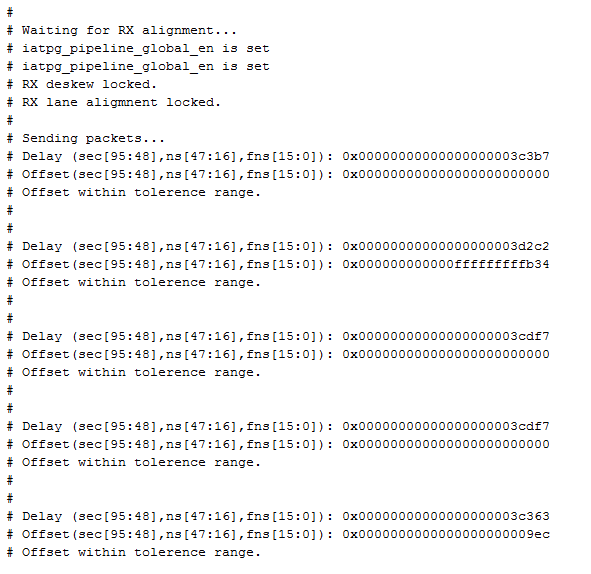
Figure 20. Sample Simulation Output for Design Example with the IEEE 1588v2 Feature (Part 2 of 2)