P-Tile Avalon® Streaming Intel® FPGA IP for PCI Express* User Guide
ID
683059
Date
10/02/2023
Public
A newer version of this document is available. Customers should click here to go to the newest version.
1. About the P-tile Avalon® Intel® FPGA IPs for PCI Express
2. IP Architecture and Functional Description
3. Advanced Features
4. Interfaces
5. Parameters
6. Testbench
7. Troubleshooting/Debugging
8. P-tile Avalon® Streaming Intel FPGA IP for PCI Express* User Guide Archives
9. Document Revision History for the P-Tile Avalon® Streaming Intel® FPGA IP for PCI Express* User Guide
A. Configuration Space Registers
B. Root Port Enumeration
C. Implementation of Address Translation Services (ATS) in Endpoint Mode
D. Packets Forwarded to the User Application in TLP Bypass Mode
E. Using the Avery BFM for Intel P-Tile PCI Express Gen4 x16 Simulations
F. Bifurcated Endpoint Support for Independent Warm Resets
G. Margin Masks for the P-Tile Avalon Streaming Intel FPGA IP for PCI Express
3.2.2.5.1. VirtIO Common Configuration Capability Register (Address: 0x012)
3.2.2.5.2. VirtIO Common Configuration BAR Indicator Register (Address: 0x013)
3.2.2.5.3. VirtIO Common Configuration BAR Offset Register (Address: 0x014)
3.2.2.5.4. VirtIO Common Configuration Structure Length Register (Address 0x015)
3.2.2.5.5. VirtIO Notifications Capability Register (Address: 0x016)
3.2.2.5.6. VirtIO Notifications BAR Indicator Register (Address: 0x017)
3.2.2.5.7. VirtIO Notifications BAR Offset Register (Address: 0x018)
3.2.2.5.8. VirtIO Notifications Structure Length Register (Address: 0x019)
3.2.2.5.9. VirtIO Notifications Notify Off Multiplier Register (Address: 0x01A)
3.2.2.5.10. VirtIO ISR Status Capability Register (Address: 0x02F)
3.2.2.5.11. VirtIO ISR Status BAR Indicator Register (Address: 0x030)
3.2.2.5.12. VirtIO ISR Status BAR Offset Register (Address: 0x031)
3.2.2.5.13. VirtIO ISR Status Structure Length Register (Address: 0x032)
3.2.2.5.14. VirtIO Device Specific Capability Register (Address: 0x033)
3.2.2.5.15. VirtIO Device Specific BAR Indicator Register (Address: 0x034)
3.2.2.5.16. VirtIO Device Specific BAR Offset Register (Address 0x035 )
3.2.2.5.17. VirtIO Device Specific Structure Length Register (Address: 0x036)
3.2.2.5.18. VirtIO PCI Configuration Access Capability Register (Address: 0x037)
3.2.2.5.19. VirtIO PCI Configuration Access BAR Indicator Register (Address: 0x038)
3.2.2.5.20. VirtIO PCI Configuration Access BAR Offset Register (Address: 0x039)
3.2.2.5.21. VirtIO PCI Configuration Access Structure Length Register (Address: 0x03A)
3.2.2.5.22. VirtIO PCI Configuration Access Data Register (Address: 0x03B)
4.1. Overview
4.2. Clocks and Resets
4.3. Serial Data Interface
4.4. Avalon-ST Interface
4.5. Hard IP Status Interface
4.6. Interrupt Interface
4.7. Error Interface
4.8. Hot Plug Interface (RP Only)
4.9. Power Management Interface
4.10. Configuration Output Interface
4.11. Configuration Intercept Interface (EP Only)
4.12. Hard IP Reconfiguration Interface
4.13. PHY Reconfiguration Interface
4.14. Page Request Service (PRS) Interface (EP Only)
4.4.1. TLP Header and Data Alignment for the Avalon-ST RX and TX Interfaces
4.4.2. Avalon® -ST RX Interface
4.4.3. Avalon® -ST RX Interface rx_st_ready Behavior
4.4.4. RX Flow Control Interface
4.4.5. Avalon® -ST TX Interface
4.4.6. Avalon® -ST TX Interface tx_st_ready Behavior
4.4.7. TX Flow Control Interface
4.4.8. Tag Allocation
5.2.3.1. Device Capabilities
5.2.3.2. VirtIO Parameters
5.2.3.3. Link Capabilities
5.2.3.4. Legacy Interrupt Pin Register
5.2.3.5. MSI Capabilities
5.2.3.6. MSI-X Capabilities
5.2.3.7. Slot Capabilities
5.2.3.8. Latency Tolerance Reporting (LTR)
5.2.3.9. Process Address Space ID (PASID)
5.2.3.10. Device Serial Number Capability
5.2.3.11. Page Request Service (PRS)
5.2.3.12. Access Control Service (ACS) Capabilities
5.2.3.13. Power Management
5.2.3.14. Vendor Specific Extended Capability (VSEC) Registers
5.2.3.15. TLP Processing Hints (TPH)
5.2.3.16. Address Translation Services (ATS) Capabilities
6.3.5.1. ebfm_barwr Procedure
6.3.5.2. ebfm_barwr_imm Procedure
6.3.5.3. ebfm_barrd_wait Procedure
6.3.5.4. ebfm_barrd_nowt Procedure
6.3.5.5. ebfm_cfgwr_imm_wait Procedure
6.3.5.6. ebfm_cfgwr_imm_nowt Procedure
6.3.5.7. ebfm_cfgrd_wait Procedure
6.3.5.8. ebfm_cfgrd_nowt Procedure
6.3.5.9. BFM Configuration Procedures
6.3.5.10. BFM Shared Memory Access Procedures
6.3.5.11. BFM Log and Message Procedures
6.3.5.12. Verilog HDL Formatting Functions
6.3.5.11.1. ebfm_display Verilog HDL Function
6.3.5.11.2. ebfm_log_stop_sim Verilog HDL Function
6.3.5.11.3. ebfm_log_set_suppressed_msg_mask Task
6.3.5.11.4. ebfm_log_set_stop_on_msg_mask Verilog HDL Task
6.3.5.11.5. ebfm_log_open Verilog HDL Function
6.3.5.11.6. ebfm_log_close Verilog HDL Function
A.3.1. Intel-Defined VSEC Capability Header (Offset 00h)
A.3.2. Intel-Defined Vendor Specific Header (Offset 04h)
A.3.3. Intel Marker (Offset 08h)
A.3.4. JTAG Silicon ID (Offset 0x0C - 0x18)
A.3.5. User Configurable Device and Board ID (Offset 0x1C - 0x1D)
A.3.6. General Purpose Control and Status Register (Offset 0x30)
A.3.7. Uncorrectable Internal Error Status Register (Offset 0x34)
A.3.8. Uncorrectable Internal Error Mask Register (Offset 0x38)
A.3.9. Correctable Internal Error Status Register (Offset 0x3C)
A.3.10. Correctable Internal Error Mask Register (Offset 0x40)
E.3. Integrate Avery BFMs (Root Complex)
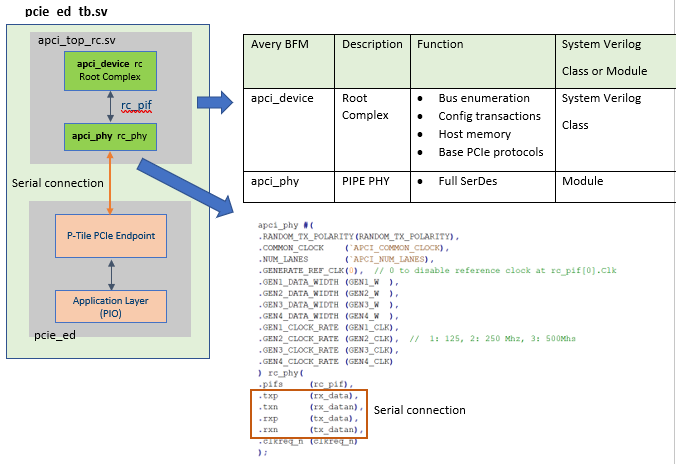
P-Tile supports serial mode connection only. The Avery Root Complex must instantiate a standalone BFM PHY to interface with the P-Tile PCIe Hard IP. The Avery BFM replaces the default Root Port BFM (dut_pcie_tb) in the P-Tile PCIe PIO example design testbench. The following diagram is a new top-level testbench, pcie_ed_tb.sv, that includes the Avery BFM.
Figure 100. Integrating the Avery BFM (Root Complex) and the PCIe Example Design
To include the Avery BFM, use the pcie_ed_tb.sv provided in the .zip file that you download or modify the example design top-level testbench as follows:
- Open the example design top-level testbench file <example design folder>/pcie_ed_tb/pcie_ed_tb/sim/pcie_ed_tb.v.
- Import Avery BFM packages by adding the following lines below the `timescale statement:
- import avery_pkg::*;
- import apci_pkg::*;
- import apci_pkg_test::*;
- `include "apci_defines.svh"
- Include the Avery BFM by adding the following line above the example design Root Port BFM (dut_pcie_tb).
- `include "./../../apci_top_rc.sv"
- Comment out the example design Root Port BFM (dut_pcie_tb).
- Save the file and rename it to pcie_ed_tb.sv.
- Open <example design folder>/pcie_ed_tb/pcie_ed_tb/sim/common/vcs_files.tcl. Find and replace pcie_ed_tb.v with pcie_ed_tb.sv.
For details, refer to apci_top_rc.sv, pcie_ed_tb.sv, and vcs_files.tcl files available in the .zip file that you download.