P-Tile Avalon® Streaming Intel® FPGA IP for PCI Express* Design Example User Guide
ID
683038
Date
4/04/2024
Public
1. About the P-tile Avalon® Streaming Intel® FPGA IP for PCI Express Design Examples
2. Quick Start Guide
3. P-tile Avalon® Streaming IP for PCI Express* Design Example User Guide Archives
4. Document Revision History for the Intel® P-Tile Avalon® Streaming Hard IP for PCIe* Design Example User Guide
2.3.2.3. SR-IOV Design Example Testbench
The figure below shows the SR-IOV design example simulation design hierarchy. The tests for the SR-IOV design example are performed by the task called sriov_test, which is defined in altpcietb_bfm_cfbp.sv.
Figure 21. SR-IOV Design Example Simulation Design Hierarchy
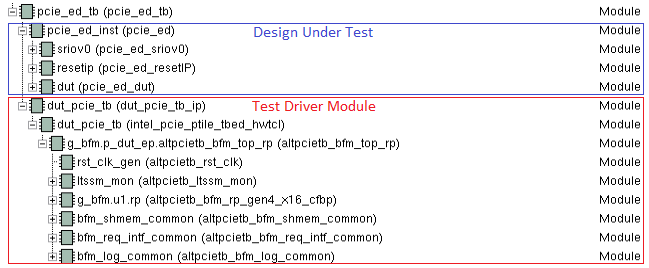
The SR-IOV testbench supports up to two Physical Functions (PFs) and 32 Virtual Functions (VFs) per PF.
The testbench starts with link training and then accesses the configuration space of the IP for enumeration. After that, it performs the following steps:
- Send a memory write request to a PF followed by a memory read request to read back the same data for comparison. If the read data matches the write data, it is a Pass. This test is performed by the task called my_test (defined in altpcietb_bfm_cfbp.v). This test is repeated twice for each PF.
- Send a memory write request to a VF followed by a memory read request to read back the same data for comparison. If the read data matches the write data, it is a Pass. This test is performed by the task called cfbp_target_test (defined in altpcietb_bfm_cfbp.v). This test is repeated for each VF.
The first memory write takes place around 263 us. It is followed by a memory read at the Avalon® -ST RX interface of PF0 of the P-tile Hard IP for PCIe. The Completion TLP appears shortly after the memory read request at the Avalon® -ST TX interface.