P-Tile Avalon® Streaming Intel® FPGA IP for PCI Express* Design Example User Guide
ID
683038
Date
4/04/2024
Public
1. About the P-tile Avalon® Streaming Intel® FPGA IP for PCI Express Design Examples
2. Quick Start Guide
3. P-tile Avalon® Streaming IP for PCI Express* Design Example User Guide Archives
4. Document Revision History for the Intel® P-Tile Avalon® Streaming Hard IP for PCIe* Design Example User Guide
2.3.2.2. PIO Design Example Testbench
The figure below shows the PIO design example simulation design hierarchy. The tests for the PIO design example are defined with the apps_type_hwtcl parameter set to 3. The tests run under this parameter value are defined in ebfm_cfg_rp_ep_rootport, find_mem_bar and downstream_loop.
Figure 20. PIO Design Example Simulation Design Hierarchy
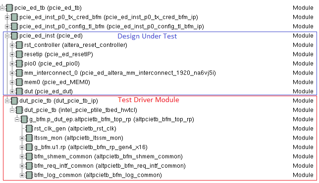
The testbench starts with link training and then accesses the configuration space of the IP for enumeration. A task called downstream_loop (defined in the Root Port PCIe BFM altpcietb_bfm_rp_gen4_x16.sv) then performs the PCIe link test. This test consists of the following steps:
- Issue a memory write command to write a single dword of data into the on-chip memory behind the Endpoint.
- Issue a memory read command to read back data from the on-chip memory.
- Compare the read data with the write data. If they match, the test counts this as a Pass.
- Repeat Steps 1, 2 and 3 for 10 iterations.
The first memory write takes place around 219 us. It is followed by a memory read at the Avalon® -ST RX interface of the P-tile Hard IP for PCIe. The Completion TLP appears shortly after the memory read request at the Avalon® -ST TX interface.