1.2. Functional Description for the Programmed Input/Output (PIO) Design Example
The PIO design example performs memory transfers from a host processor to a target device. In this example, the host processor requests single-dword MemRd and MemWr TLPs.
The PIO design example automatically creates the files necessary to simulate and compile in the Quartus® Prime software. The design example covers a wide range of parameters. However, it does not cover all possible parameterizations of the P-Tile Hard IP for PCIe.
This design example includes the following components:
- The generated P-Tile Avalon Streaming Hard IP Endpoint variant (DUT) with the parameters you specified. This component drives TLP data received to the PIO application.
- The PIO Application (APPS) component, which performs the necessary translation between the PCI Express TLPs and simple Avalon-MM writes and reads to the on-chip memory.
- An on-chip memory (MEM) component. For the 1x16 design example, the on-chip memory consists of one 16 KB memory block. For the 2x8 design example, the on-chip memory consists of two 16 KB memory blocks.
- Reset Release IP: This IP holds the control circuit in reset until the device has fully entered user mode. The FPGA asserts the INIT_DONE output to signal that the device is in user mode. The Reset Release IP generates an inverted version of the internal INIT_DONE signal to create the nINIT_DONE output that you can use for your design.The nINIT_DONE signal is high until the entire device enters user mode. After nINIT_DONE asserts (low), all logic is in user mode and operates normally. You can use the nINIT_DONE signal in one of the following ways:
- To gate an external or internal reset.
- To gate the reset input to the transceiver and I/O PLLs.
- To gate the write enable of design blocks such as embedded memory blocks, state machine, and shift registers.
- To synchronously drive register reset input ports in your design.
The simulation testbench instantiates the PIO design example and a Root Port BFM to interface with the target Endpoint.
Figure 1. Block Diagram for the Platform Designer PIO 1x16 Design Example Simulation Testbench
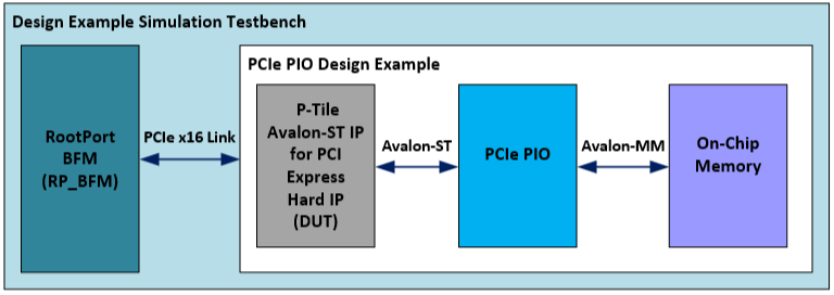
Figure 2. Block Diagram for the Platform Designer PIO 2x8 and 1x8 Design Example Simulation Testbench
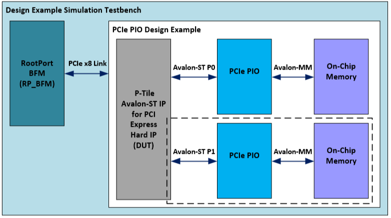
Note: In Figure 2 above, the second PCIe x8 link (the block in the dotted line) is not present in the simulation testbench and hardware design for the PIO 1x8 design example.
Note: The simulation testbench for the PCIe 2x8 PIO design example above is configured for a single PCIe x8 link although the actual design implements two PCIe x8 links.
The test program writes to and reads back data from the same location in the on-chip memory. It compares the data read to the expected result. The test reports, "Simulation stopped due to successful completion" if no errors occur.
The P-Tile Avalon® Streaming design example supports the following configurations:
- Gen4 x16 512-bit Endpoint
- Gen3 x16 512-bit Endpoint
- Gen3 x16 256-bit Endpoint
- Gen4 x8x8 512-bit (250 MHz or below) Endpoint
- Gen4 x8x8 256-bit Endpoint
- Gen3 x8x8 256-bit Endpoint
- Gen4 x8 256-bit (350 MHz or above) Endpoint
- Gen3 x8 256-bit Endpoint
Note: This design example only supports the default settings in the Parameter Editor of the P-tile Avalon® Streaming IP for PCI Express.
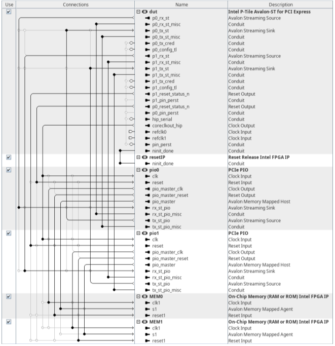
Figure 3. Platform Designer System Contents for P-Tile Avalon® Streaming PCI Express 1x16 and 1x8 PIO Design Example The Platform Designer generates this design for up to Gen4 1x16 or 1x8 variants.
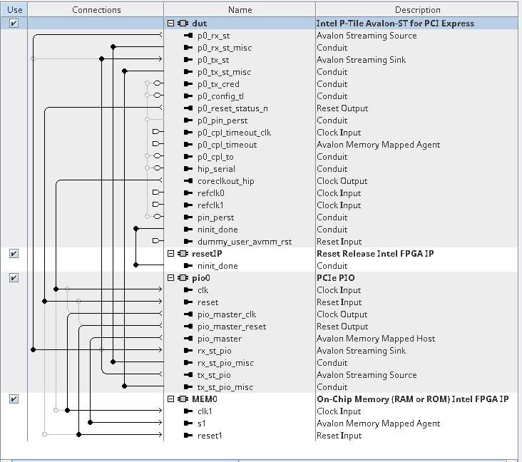
Figure 4. Platform Designer System Contents for P-Tile Avalon® Streaming PCI Express 2x8 PIO Design ExampleThe Platform Designer generates this design for up to Gen4 x8x8 variants.