Due to a problem in the Intel® Quartus® Prime Pro Edition Software version 22.1, the F-Tile SDI II Intel® FPGA IP parallel loopback with external VCXO Design Example has higher jitter than required by the SD-SDI video standard due to the FVH sync signal output from the SDI RX core not being an acceptable source to clock the external VCXO on the daughter card required to synchronize the clock between TX and RX. This problem impacts triple-rate and multi-rate SDI video standard, as SD-SDI is part of the supported standard. This problem will also impact any Intel Agilex® 7 FPGA designs that follow this Intel implementation of the VCXO with TI LMH1983 chip in their design.
To work around this problem, use one of two possible solutions:
1. Use F-Tile SDI II Intel® FPGA IP parallel loopback without external VCXO Design Example. This design supports triple-rate and multi-rate SDI video standard (including SD-SDI), while using internal PLL to synchronize the clock between TX and RX.
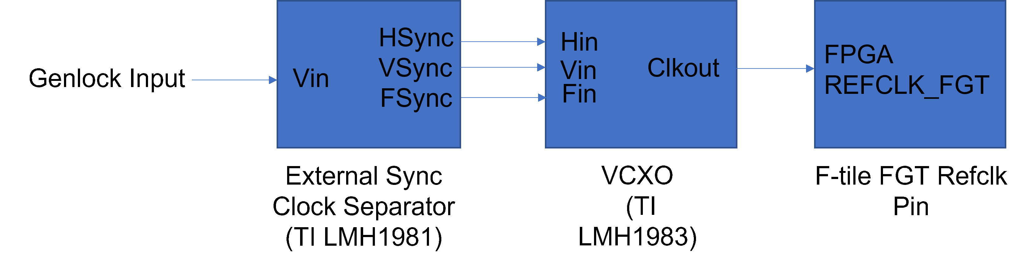
2. Use an external sync clock separator chip such as the TI LMH1981, to generate the FVH timing signal and feed the signals to the external VCXO (TI LMH1983) as shown in Figure 1. The TI LMH1981 external clock separator is available on the Nextera and Terasic 12G SDI-FMC daughter card and user has to supply the genlock input to the TI LMH1981 accordingly.
Figure 1.