In the Quartus® Prime Pro Edition Software, you may see that the phase-locked loop (PLL) clocks are not correctly derived when the PLL reference clock has multiple master clocks. This occurs because the Timing Analyzer cannot identify which of the multiple master clocks should be used.
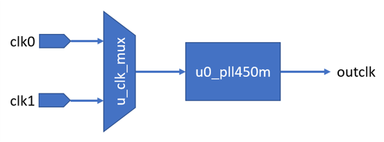
You might see the warning messages shown below in the Timing Analyzer when the clock scheme is as follows:
Warning(332036): Clock: clk0 found as a potential master clock candidate
Warning(332036): Clock: clk1 found as a potential master clock candidate
Warning(332087): The master clock for this clock assignment could not be derived. Clock: u0_pll450m|iopll_0_n_cnt_clk was not created.
Warning(332036): Clock: clk0 found as a potential master clock candidate
Warning(332036): Clock: clk1 found as a potential master clock candidate
Warning(332087): The master clock for this clock assignment could not be derived. Clock: u0_pll450m|iopll_0_m_cnt_clk was not created.
Warning(332036): Clock: clk0 found as a potential master clock candidate
Warning(332036): Clock: clk1 found as a potential master clock candidate
Warning(332087): The master clock for this clock assignment could not be derived. Clock: u0_pll450m|iopll_0_outclk0 was not created.
This only occurs in designs targetting Stratix® 10 devices and Agilex™ devices.
To correctly constrain the PLL output clocks, manually generate the master clocks, specify the master clock for each PLL output clock and add clock groups to cut the PLL output clocks from different reference clocks.
The following timing constraints can be used for the clock scheme above:
create_clock -name clk0 -period 100MHz [get_ports clk0]
create_clock -name clk1 -period 100MHz [get_ports clk1]
create_generated_clock -name {u0|iopll_0_m_cnt_clk} -source {u0_pll450m|iopll_0|tennm_pll|core_refclk} -divide_by 12 -multiply_by 1 -duty_cycle 50.00 -master {clk0} { u0_pll450m|iopll_0|tennm_pll~mcntr_reg } -add
create_generated_clock -name {u0|iopll_0_n_cnt_clk} -source {u0_pll450m|iopll_0|tennm_pll|core_refclk} -divide_by 1 -multiply_by 1 -duty_cycle 50.00 -master {clk0} { u0_pll450m|iopll_0|tennm_pll~ncntr_reg } -add
create_generated_clock -name {u0|iopll_0_outclk0} -source {u0_pll450m|iopll_0|tennm_pll|core_refclk} -divide_by 3 -multiply_by 12 -duty_cycle 50.00 -master {clk0} { u0_pll450m|iopll_0|tennm_pll|outclk[1] } -add
create_generated_clock -name {u1|iopll_0_m_cnt_clk} -source {u0_pll450m|iopll_0|tennm_pll|core_refclk} -divide_by 12 -multiply_by 1 -duty_cycle 50.00 -master {clk1} { u0_pll450m|iopll_0|tennm_pll~mcntr_reg } -add
create_generated_clock -name {u1|iopll_0_n_cnt_clk} -source {u0_pll450m|iopll_0|tennm_pll|core_refclk} -divide_by 1 -multiply_by 1 -duty_cycle 50.00 -master {clk1} { u0_pll450m|iopll_0|tennm_pll~ncntr_reg } -add
create_generated_clock -name {u1|iopll_0_outclk0} -source {u0_pll450m|iopll_0|tennm_pll|core_refclk} -divide_by 3 -multiply_by 12 -duty_cycle 50.00 -master {clk1} { u0_pll450m|iopll_0|tennm_pll|outclk[1] } -add
set_clock_groups -exclusive -group {u0|iopll_0_outclk0} -group {u1|iopll_0_outclk0}
You can get the correct node name in the node finder, and the divider and multiplier parameters from the PLL configuration.