This topic prints best in Landscape orientation.
Displays the minimized equations for all logic in the project.
The equations, which represent the results of extensive logic synthesis, are provided as reference information. Because logic synthesis minimizes the logic required to implement a design, redundant or unnecessary logic in the original design files may not appear in this report.
A node name in the equation can have any one of the following formats:
|
Format Note (1) |
Description |
Example |
|---|---|---|
|
<Name> |
Used for the input and output pins of the current design entity. This format is also used on buried node names in the design entity when the same buried node name remains following compilation. Synthesized names, however, are not used. |
updown |
|
<Entity> <Instance>_<Name> |
Used for nodes in hierarchy levels below the current design entity where you assigned names to the nodes. The hierarchy level is represented by <Entity> <Instance>. |
B1_carrybit[3] |
|
<Entity> <Instance> <Type> <Index>[Q] |
Used for nodes that are created or synthesized during compilation. |
B1L7Q or C3M5 |
|
<Any One of the Above Formats>_EQ[<nn>] |
Used for nodes to which you assigned a temporary name. The name is formed by adding the suffix, _EQ[<nn>], to one of the other formats. |
B1_carrybit[8]_EQ4 |
Equations include the following components:
|
Component |
Description |
|---|---|
|
CASCADE |
Represents a CASCADE buffer inserted by Analysis & Synthesis. |
|
CARRY |
Represents the CARRY output of a CARRY_SUM buffer. |
|
SUM |
Represents the SUM output of a CARRY_SUM buffer. |
|
DFFE |
Represents a DFFE. <Qoutput>=DFFE ( <Dinput>,<clock>,<nclear>,<npreset>,<clockenable> ). |
|
DFFEA |
Represents a DFFEA. <Qoutput>=DFFEA ( <Dinput>,<clock>,<nclear>,<npreset>,<clockenable>,<data>,<aload> ). |
|
DFFEAS |
Represents a DFFEAS. <Qoutput>=DFFEAS ( <Dinput>,<clock>,<nclear>,<npreset>,<clockenable>,<asdata>,<aload>,<sclear>,<sload> ). |
|
GXB_RX |
Represents GXB receiver channel usage in supported device(ArriaIIseries, and StratixIV) families. <node> = GXB_RX. <output port> (.DATAIN( <node> ), .XGMDATAIN( <node> ), .MASTERCLK( <node> ), .CORECLK( <node> ), .CRUCLK( <node> ), .PLLCLK( <node> ), .SOFTRESET( <node> ), .SERIALFBK( <node> ), .SLPBK( <node> ), .BITSLIP( <node> ), .ENACDETECT( <node> ), .WRITEENABLE( <node> ), .READENABLE( <node> ), .ALIGNSTATUS( <node> ), .DISABLEFIFORDIN( <node> ), .DISABLEFIFOWRIN( <node> ), .FIFORDIN( <node> ), .ENABLEDESKEW( <node> ), .FIFORESETRD( <node> ), .XGMCTRLIN( <node> ), .PARALLELFBK( <node> ), .POST8B10B( <node> ). |
|
GXB_TX |
Represents GXB transmitter channel usage in supported device(ArriaIIseries, and StratixIV) families. <node> = GXB_TX. <output port> (.DATAIN( <node> ), .SERIALDATAIN( <node> ), .XGMDATAIN( <node> ), .CORECLK( <node> ), .PLLCLK( <node> ), .FASTPLLCLK( <node> ), .SOFTRESET( <node> ), .XGMCTRL( <node> ), .SLPBK( <node> ), .CTRLENABLE( <node> ), .FORCEDISPARITY( <node> ). |
|
MEMORY |
Represents memory in supported device(ArriaIIseries, and StratixIV) families. <data output> = MEMORY ( <port A data input>, <port B data input>, <port A address>, <port B address>, <port A write enable>, <port B read/write enable>, <port A byte mask>, <port B byte mask>, <clock0>, <clock1>, <clock enable0>, <clock enable1>, <clear0>, <clear1> ). |
|
MEMORY_SEGMENT |
Represents memory in supported device(CycloneIII, and CycloneIV) families. <data output> = MEMORY_SEGMENT ( <clock0>, <clock1>, <clock enable0>, <clock enable1>, <write enable0>, <read enable>, <clear0>, <clear1> <data input>, <write address>, <read address> ). |
|
PLL |
Represents fast and enhanced PLL usage in supported device(ArriaIIseries) families. <node> = PLL. <output port> (.FBIN( <node> ),.ENA( <node> ),.CLKSWITCH( <node> ), .ARESET( <node> ),.PFDENA( <node> ), .SCANCLK( <node> ), .SCANACLR( <node> ) , .SCANDATA( <node> ) , .COMPARATOR( <node> ),.INCLK( <node> ),.INCLK( <node> ),.CLKENA( <node> ), .CLKENA( <node> ),.CLKENA( <node> ),.CLKENA( <node> ),.CLKENA( <node> ),.CLKENA( <node> ), .EXTCLKENA( <node> ), .EXTCLKENA( <node> ),.EXTCLKENA( <node> ), .EXTCLKENA( <node> )). |
|
SERDES_RX |
Represents a SERDES receiver. <node> = SERDES_RX. <data output> (.DATAIN( <node> ), .CLK0( <node> ), .ENABLE0( <node> ), .ENABLE1( <node> )). |
|
SERDES_TX |
Represents a SERDES transmitter. <node> = SERDES_TX. <data output> (.DATAIN( <node> ), .CLK0( <node> ), <data input> ). |
|
INPUT |
Represents the input pin. <pin name> = INPUT (). |
|
OUTPUT |
Represents the output pin. <pin name> = OUTPUT ( <node> ). |
|
BIDIR |
Represents the bidirectional pin. <pin name> = BIDIR ( <node> ). |
|
TRI_BUS |
Represents a tri-state bus that is made up of multiple inputs, any one of which drives a net output. |
|
TRI |
Represents a tri-state node. <pin name> = TRI ( <input>, <output enable> ). |
|
GLOBAL |
Represents a global signal driven by a dedicated input pin or internal logic. <pin name> = GLOBAL ( <node> ). |
|
MUX |
Represents a 2:1 MUX. <Q output> = MUX ( <data0>, <data1>, <select>, <enable> ). |
|
CARRY_SUM |
Represents a CARRY_SUM buffer. |
|
LATCH |
Represents a latch. <Q output> = LATCH ( <D input>, <latch enable> ). |
|
ROUND |
Represents the output of a rounding operation. |
|
SATURATE |
Represents the output of a saturation operation. |
|
DYNAMIC |
Represents the output of a DSP block in DYNAMIC mode. |
|
APPEND_ZEROS_TO_END |
Represents the output of an operation that appends zeros to the end of an input. |
|
& |
AND operator. |
|
$ |
XOR (exclusive OR) operator. |
|
# |
OR operator. |
|
! |
NOT operator. |
|
SUM(val) |
Represents the sum result of an addition operation. val is a sub equation representing the + result and is assigned to the sumout port. |
|
SHARE(val) |
Represents a value passed through a shared arithmetic connection. |
|
DELAY_! BUFFER |
Represents the DQS delay buffer in StratixIII. delayed_dqs_signal = DELAY_BUFFER (<dqs_signal>, <dqs update enable control>, <delay control setting>, <offset control setting>). |
|
DDIO_IN_H |
Represents the output sampled data of the input double data rate signal at the rising edge of the input clock. <sampled data signal during the rising edge of the clock> = DDIO_IN_H (<input double data-rate signal>, <clock>, <clock enable>, <asynchronous reset>). |
|
DDIO_IN_L |
Represents the output sampled data of the input double data-rate signal at the falling edge of the input clock. <sampled data signal during the falling edge of the clock> = DDIO_IN_H (<input double data-rate signal>, <clock>, <clock enable>, <asynchronous reset>). |
|
DDIO_OE |
Represents the output enable signal for a double data-rate output/bidir pin. <ddio output-enable signal> = DDIO_OE(<output enable source>, <clock>, <preset>, <clock enable>) |
Each equation or set of equations is preceded by comments describing the node name, the node source if from a text-based design file, and node location. For example:
--B1_carrybit[8] is |LPM_COUNTER:inst1|carrybit[8] at LC8_1_A1
The following example shows a portion of the Equations report for a sample design:
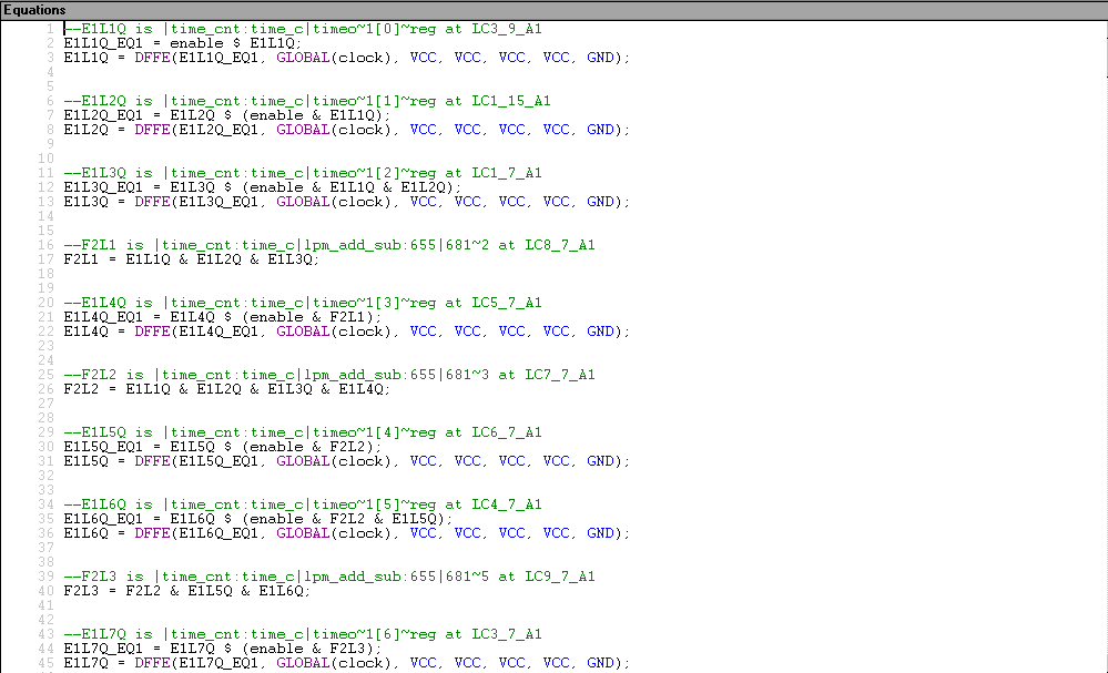
Legend:
- Single-line comments Green
- Keywords Blue
- Reserved identifiers (AHDL) Dark Purple
- Synthesized logic cells: Names that include ~ characters.