External Memory Interfaces (EMIF) IP User Guide: Agilex™ 3 FPGAs and SoCs
3.5.2. Advanced: Memory Timing Tab
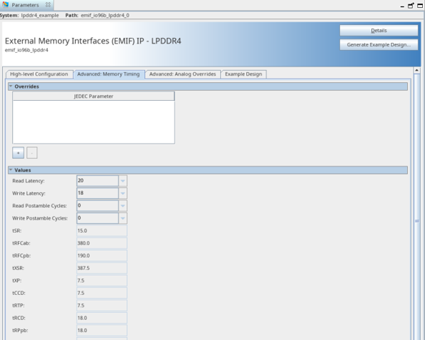
This tab contains two groups of parameters: Overrides and Values. The tables which follow provide descriptions of the parameters on this tab.
| Parameter Name | Description |
|---|---|
| JEDEC Parameter | Name of JEDEC Parameter to explicitly override; the values will be applied and appear in the list below. Default value is Legal values are: MEM_CL_CYC, MEM_CWL_CYC, MEM_RD_POSTAMBLE_CYC, MEM_WR_POSTAMBLE_CYC, MEM_TSR_NS, MEM_TRFCAB_NS, MEM_TRFCPB_NS, MEM_TXSR_NS, MEM_TXP_NS, MEM_TCCD_NS, MEM_TRTP_NS, MEM_TRCD_NS, MEM_TRPPB_NS, MEM_TRPAB_NS, MEM_TRAS_NS, MEM_TWR_NS, MEM_TWTR_NS, MEM_TRRD_NS, MEM_TPPD_CYC, MEM_TFAW_NS, MEM_TRC_NS, MEM_TREFW_NS, MEM_MINNUMREFSREQ, MEM_TREFI_NS, MEM_TCKE_NS, MEM_TCMDCKE_NS, MEM_TCKELCK_NS, MEM_TCSCKE_NS, MEM_TCKCKEH_NS, MEM_TCSCKEH_NS, MEM_TMRWCKEL_NS, MEM_TZQCKE_NS, MEM_TMRR_NS, MEM_TMRW_NS, MEM_TMRD_NS, MEM_TESCKE_NS, MEM_TZQCAL_NS, MEM_TZQLAT_NS, MEM_TDQSCK_MAX_NS, MEM_TDQSCK_MIN_NS, MEM_TCKCKEL_NS, MEM_TCKELCMD_NS, MEM_TCKEHCMD_NS (Identifier: JEDEC_OVERRIDE_TABLE_PARAM_NAME) |
| Parameter Name | Description |
|---|---|
| Read Latency | Read Latency of the memory device in clock cycles. (Identifier: MEM_CL_CYC) |
| Write Latency | Write Latency in clock cycles. (Identifier: MEM_CWL_CYC) |
| Read Postamble Cycles | Duration of read postamble in cycles. (Identifier: MEM_RD_POSTAMBLE_CYC) |
| Write Postamble Cycles | Duration of write postamble in cycles. (Identifier: MEM_WR_POSTAMBLE_CYC) |
| tSR | Minimum duration (Entry to Exit) of Self Refresh in nanoseconds. (Identifier: MEM_TSR_NS) |
| tRFCab | All-Bank Refresh Cycle Time in nanoseconds. (Identifier: MEM_TRFCAB_NS) |
| tRFCpb | Per-Bank Refresh Cycle Time in nanoseconds. (Identifier: MEM_TRFCPB_NS) |
| tXSR | Self-Refresh Exit to Next Valid Command Delay Time in nanoseconds. (Identifier: MEM_TXSR_NS) |
| tXP | Exit Power-Down to Next Valid Command Delay Time in nanoseconds. (Identifier: MEM_TXP_NS) |
| tCCD | CAS-to-CAS Delay in nanoseconds. (Identifier: MEM_TCCD_NS) |
| tRTP | Internal READ to PRECHARGE Command Delay Time in nanoseconds. (Identifier: MEM_TRTP_NS) |
| tRCD | RAS-to-CAS Delay in nanoseconds. (Identifier: MEM_TRCD_NS) |
| tRPpb | Per-Bank Precharge Time in nanoseconds. (Identifier: MEM_TRPPB_NS) |
| tRPab | All-Bank Precharge Time in nanoseconds. (Identifier: MEM_TRPAB_NS) |
| tRAS | Row Active Time in nanoseconds. (Identifier: MEM_TRAS_NS) |
| tWR | Write Recovery Time in nanoseconds. (Identifier: MEM_TWR_NS) |
| tWTR | Write-to-Read Delay in nanoseconds. (Identifier: MEM_TWTR_NS) |
| tRRD | RAS-to-RAS (Active Bank-A to Active Bank-B) Delay Time in nanoseconds. (Identifier: MEM_TRRD_NS) |
| tFAW | Four-bank ACTIVE window time in nanoseconds. (Identifier: MEM_TFAW_NS) |
| tRC | Activate-to-Activate command period (same bank) in nanoseconds. (Identifier: MEM_TRC_NS) |
| tREFW | Refresh window time in nanoseconds. (Identifier: MEM_TREFW_NS) |
| Min Number of Refs Reqd | Minimum Number of Refreshes Required. (Identifier: MEM_MINNUMREFSREQ) |
| tREFI | Refresh Interval Time in nanoseconds. (Identifier: MEM_TREFI_NS) |
| tCKE | CKE Minimum Pulse Width time in nanoseconds. (Identifier: MEM_TCKE_NS) |
| tCMDCKE | Delay from valid command to power-down-entry (CKE low) in nanoseconds. (Identifier: MEM_TCMDCKE_NS) |
| tCKELCK | Valid clock requirement after power-down-entry in nanoseconds. (Identifier: MEM_TCKELCK_NS) |
| tCSCKE | Valid CS requirement before power-down-entry (CKE low) in nanoseconds. (Identifier: MEM_TCSCKE_NS) |
| tCKCKEH | Valid clock requirement before power-down-exit in nanoseconds. (Identifier: MEM_TCKCKEH_NS) |
| tCSCKEH | Valid CS requirement before power-down-exit (CKE high) in nanoseconds. (Identifier: MEM_TCSCKEH_NS) |
| tMRWCKEL | Delay from MRW command to power-down-entry (CKE low) in nanoseconds. (Identifier: MEM_TMRWCKEL_NS) |
| tZQCKE | Delay from ZQCal Start command to power-down-entry (CKE low) in nanoseconds. (Identifier: MEM_TZQCKE_NS) |
| tMRR | Mode Register Read Command Period Time in nanoseconds. (Identifier: MEM_TMRR_NS) |
| tMRW | Mode Register Write Command Period Time in nanoseconds. (Identifier: MEM_TMRW_NS) |
| tMRD | Mode Register Set Command Period Time in nanoseconds. (Identifier: MEM_TMRD_NS) |
| tESCKE | Delay from SRE command to CKE Input low in nanoseconds. (Identifier: MEM_TESCKE_NS) |
| tZQCAL | ZQ calibration time in nanoseconds. (Identifier: MEM_TZQCAL_NS) |
| tZQLAT | ZQcal Latch time in nanoseconds. (Identifier: MEM_TZQLAT_NS) |
| tDQSCK_MAX | Maximum DQS output access time from CK in nanoseconds. (Identifier: MEM_TDQSCK_MAX_NS) |
| tDQSCK_MIN | Minimum DQS output access time from CK in nanoseconds. (Identifier: MEM_TDQSCK_MIN_NS) |
| tCKCKEL | Clock valid requirements after power-down-entry (CKE low) in nanoseconds. (Identifier: MEM_TCKCKEL_NS) |
| tCKELCMD | Valid command requirement after CKE input low in nanoseconds. (Identifier: MEM_TCKELCMD_NS) |
| tCKEHCMD | Valid command requirement after CKE input high in nanoseconds. (Identifier: MEM_TCKEHCMD_NS) |