Hyperflex® Architecture High-Performance Design Handbook
ID
683353
Date
7/07/2025
Public
Answers to Top FAQs
1. Hyperflex® FPGA Architecture Introduction
2. Hyperflex® Architecture RTL Design Guidelines
3. Compiling Hyperflex® Architecture Designs
4. Design Example Walk-Through
5. Retiming Restrictions and Workarounds
6. Optimization Example
7. Hyperflex® Architecture Porting Guidelines
8. Appendices
9. Hyperflex® Architecture High-Performance Design Handbook Archive
10. Hyperflex® Architecture High-Performance Design Handbook Revision History
2.4.2.1. High-Speed Clock Domains
2.4.2.2. Restructuring Loops
2.4.2.3. Control Signal Backpressure
2.4.2.4. Flow Control with FIFO Status Signals
2.4.2.5. Flow Control with Skid Buffers
2.4.2.6. Read-Modify-Write Memory
2.4.2.7. Counters and Accumulators
2.4.2.8. State Machines
2.4.2.9. Memory
2.4.2.10. DSP Blocks
2.4.2.11. General Logic
2.4.2.12. Modulus and Division
2.4.2.13. Resets
2.4.2.14. Hardware Re-use
2.4.2.15. Algorithmic Requirements
2.4.2.16. FIFOs
2.4.2.17. Ternary Adders
5.2.1. Insufficient Registers
5.2.2. Short Path/Long Path
5.2.3. Fast Forward Limit
5.2.4. Loops
5.2.5. One Critical Chain per Clock Domain
5.2.6. Critical Chains in Related Clock Groups
5.2.7. Complex Critical Chains
5.2.8. Extend to locatable node
5.2.9. Domain Boundary Entry and Domain Boundary Exit
5.2.10. Critical Chains with Dual Clock Memories
5.2.11. Critical Chain Bits and Buses
5.2.12. Delay Lines
2.2.7.3.1. Implementing Clock Gating
To implement clock gating, you access the USER_CLKGATE signal by use of the following IP available in the Quartus® Prime software:
- Reset Release IP—holds your design in reset until configuration is complete by gating clocks, resets, or write enables. This IP outputs the nINIT_DONE signal. When nINIT_DONE is low, the device is no longer in configuration mode.
- Clock Control IP—uses the inverted nINIT_DONE signal as a clock enable signal.
Follow these steps to implement clock gating:
- Open a design in the Quartus® Prime software.
- In IP Catalog, type reset release in the search field, and double-click the Reset Release IP .
- Specify appropriate parameters for your configuration in the parameter editor, and then click Generate HDL.
- Repeat steps 2 and 3 to add the Clock Control IP to your project. Prior to IP generation, specify the following options for the IP in the parameter editor:
- Under Clock Gating, turn on the Clock Enable option.
- For Clock Enable Type, select Root Level.
- For Enable Register Mode, select Negative Latch.
- Connect the Reset Release and Clock Control IP together:
- To gate the clocks, use inverted nINIT_DONE as the enable input to the Clock Control IP.
- If initial conditions are required, Altera recommends that the Clock Control IP also use root clock gating.
The following figure shows proper connections between the Reset Release and Clock Control IP to ensure accurate initial conditions after configuration:
Figure 19. Connections between the Reset Release (reset_release) and Clock Control (clock_control) IP Cores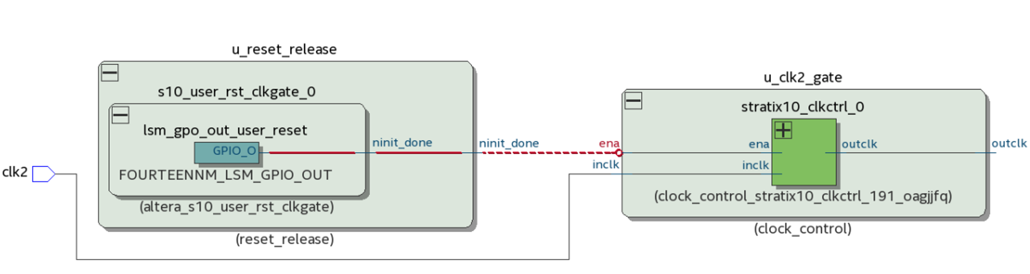
The Clock Control IP uses the ena signal to perform the clock gating function. The clock signal on the output of the Clock Control IP is then safe for use with the initialized registers (ALM and Hyper-Registers).