1.2. Generating the Design
Figure 3. Procedure
Follow these steps to generate the design example and testbench:
- In the Quartus® Prime Pro Edition software, click File > New Project Wizard to create a new Quartus® Prime project, or click File > Open Project to open an existing Quartus® Prime project. The wizard prompts you to specify a device.
- Specify the device family Agilex™ 7 and select device with F-Tile for your design.
- In the IP Catalog, locate and double-click F-Tile Interlaken IP. The New IP Variant window appears.
- Specify a top-level name <your_ip> for your custom IP variation. The parameter editor saves the IP variation settings in a file named <your_ip>.ip.
- Click OK. The parameter editor appears.
Figure 4. Example Design Tab
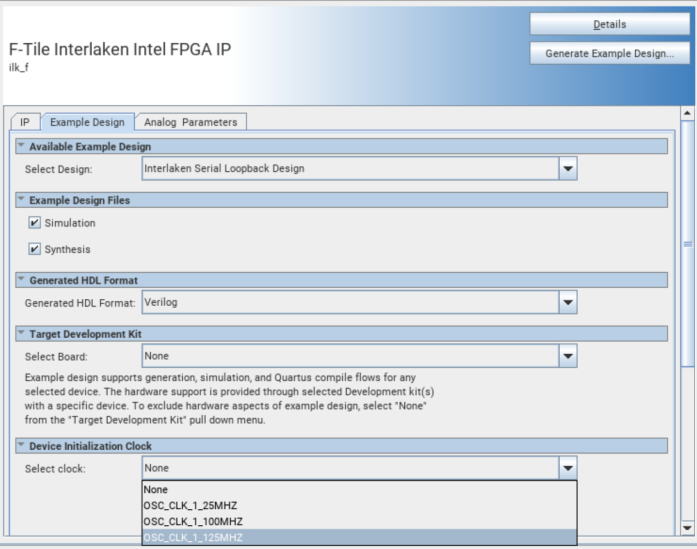
- On the IP tab, specify the parameters for your IP core variation.
- On the Example Design tab, select the Simulation option to generate the testbench. Select the Synthesis option to generate the hardware design example. You must select at least one of the Simulation and Synthesis options to generate the design example.
- For Generated HDL Format, both Verilog and VHDL option is available.
- For Target Development Kit, select the Agilex 7 FPGA I-Series Transceiver-SoC Development Kit (Production 1 4x F-Tiles) or Agilex 7 FPGA I-Series Transceiver-SoC Development Kit (Production 2 4x F-Tiles).
Note: When you select the Target Development Kit, the pin assignments are set according to the Agilex 7 FPGA I-Series Transceiver-SoC Development Kit device part number and may differ from your selected device. If you intend to test the design on hardware on a different PCB, select the None option and make the appropriate pin assignments in the .qsf file
- Select the Device Initialization Clock.
The Agilex 7 FPGA I-Series Transceiver-SoC Development Kit only supports OSC_CLK_1_125MHZ
- Click Generate Example Design. The Select Example Design Directory window appears.
- If you want to modify the design example directory path or name from the defaults displayed (ilk_f_0_example_design), browse to the new path and type the new design example directory name.
- Click OK.
Note:
In the F-Tile Interlaken IP design example, a SystemPLL is instantiated automatically, and connected to F-Tile Interlaken IP. The SystemPLL hierarchy path in the design example is:
example_design.test_env_inst.test_dut.dut.pllThe SystemPLL in the design example shares the same 156.26 MHz reference clock as the Transceiver.
Note: Very Short Reach (VSR) mode setting is added to the Design Example .qsf file to be used along with Agilex™ 7 I-Series Transceiver-SoC Development Kit. You must remove the VSR mode setting if it does not apply to your application.