A design should not contain nodes where a clock signal source (for example, an input clock pin) drives the design's registers in one of the following ways:
- The clock signal source drives registers that have clock inputs that trigger on the positive edge of the clock, and other cascaded registers that have clock inputs that trigger on the negative edge of the clock.
- The clock signal source drives only cascaded registers that have clock inputs that all trigger on either the positive or negative edge of the clock, but the design inverts the clock before driving some of the registers.
The following image shows an example where a clock signal source drives a cascaded register triggered by different clock edges:
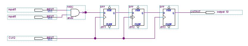
These connections can cause various design problems. Synchronous resetting may not be possible because registers are not clocked on the same edge in the design. When a design inverts the clock, additional design problems may occur; for example, the inverted clock may be mapped to regular logic or may not contain the correct time relationship to the original clock.
The registers that synchronize combinational logic that is used as a clock or reset signal are sometimes triggered by different clock edges. However, these registers do not cause problems in the design.