This paper discusses the new features and enhancements available in the 4th Gen Intel Xeon processors (formerly codenamed Sapphire Rapids) and how developers can take advantage of them. The 10nm enhanced SuperFin processor provides core microarchitecture changes and new technologies including the third generation of Intel® Optane™ DC persistent memory, on-die accelerators, Compute Express Link™ (CXL™), and more. Data center workloads can benefit from the increased core count, increased instructions per cycle, increased Intel® UPI GT/s, increased processor cache sizes, increased memory MT/s, and additional PCI Express and CXL lanes.
The table below provides a comparison between the third and fourth generation of the Intel Xeon Scalable processor family. The fourth generation builds on features found in the third generation. New capabilities/changes relative to the previous generation are in Bolded Italic. Note that the table below reflects the top capabilities for each category. There are many models of processors available with different feature combinations.
Table 1. The Next-Generation Intel Xeon Scalable Processor Family Microarchitecture Overview
| 3rd Generation Intel® Xeon® Scalable processor family with Intel® C620A series chipset | 4th Gen Intel Xeon Scalable processor family with Intel® C741 series chipset | ||
| Socket Count | 1 and 2 | 4 and 8 glue less | 1S, 2S, 4S, & glueless 8S (>8S via xNC support) |
| Die Size | 10nm | 14nm | 10nm (enhanced SuperFin) |
| Processor Core Count | Up to 40 cores (80 cores with Intel® Hyper-Threading Technology (Intel® HT Technology)) per socket | Up to 28 cores (56 cores with Intel® Hyper-Threading Technology (Intel® HT Technology)) per socket | Up to 60 cores (120 cores with Intel® Hyper-Threading Technology (Intel® HT Technology)) per socket |
| Cache |
|
|
|
| Socket Type | Socket P+ | Socket E | |
| TDP | Up to 270W | Up to 250W | Up to 350W |
| New Features | Intel® Resource Director Technology (Intel® RDT), Intel® SST-BF on select skus, Intel® Volume Management Device (Intel® VMD) 2.0, Intel® Advanced Vector Extensions 512 (Intel® AVX-512), Intel® Deep Learning Boost (Intel® DL Boost), VBMI, Intel® Speed Select Technology - Core Power (Intel® SST-CP), Intel® Speed Select Technology - Turbo Frequency (Intel® SST-TF) and enhanced Intel® Speed Select Technology - Performance Profile (Intel® SST-PP) on select skus, Intel® VROC 7.5, Intel® PFR, Converged Boot Guard and Intel TXT, Crypto Enhancements: (2xAES, SHA Extensions, VPMADD52), Intel® Software Guard Extensions (Intel® SGX), Intel® Total Memory Encryption (Intel® TME) with 64 keys, Intel® Volume Management Device 2.0, PECI 4.0, enhanced power management features. | BFLOAT16, Intel® PFR, Intel® SST-TF on select skus, next generation of Intel® Virtual RAID on CPU (Intel® VROC), Converged Intel® Boot Guard and Intel® Trusted Execution Technology (Intel® TXT) | Intel® AMX (INT8 & BFLOAT16), Intel® Advanced Vector Extensions 512 (Intel® AVX-512) (new FP16 data type), Intel® Total Memory Encryption (Intel® TME) with 128 keys, Next-Gen Intel® Quick Assist Technology (Intel® QAT), Intel® DLB, Intel® DSA, Intel® In-Memory Analytics Accelerator (Intel® IAA) |
| Physical/Virtual address bits | 52/57 | 46/48 | 52/57 |
| Memory controllers / Sub-Numa clusters | 4 / 2 | 2 / 2 | 4 / 4 |
| Memory DDR4 |
|
|
|
| Intel® Optane™ memory support | 2nd Gen Intel Optane DC persistent memory module (DDRT, In-Tile Mode, and App Direct) up to 512GB | 3rd Gen Intel Optane DC persistent memory module (DDRT2, X-Tile Mode, and Cached App Direct) up 512GB | |
| Number of Intel® Ultra Path Interconnect (Intel® UPI) Interconnects | Up to 3 links per CPU (x20 wide) | Up to 6 links per CPU (x20 wide) | Up to 4 links per CPU (x24 wide) |
| Intel® UPI Interconnect Speed | Up to 11.2 GT/s | Up to 10.4 GT/s | Up to 16 GT/s |
| PCIe |
|
|
|
| Chipset Features |
|
Enhanced Serial Peripheral Interface (eSPI) | |
|
|
||
Intel® Optane™ persistent memory 300 series
The next generation of Intel® Optane™ persistent memory modules are a form of large capacity memory that can function in either a volatile or non-volatile state and provides a new tier positioned between DRAM and storage. Traditional memory in computer architecture is volatile. The content of volatile memory is only able to exist so long as the system supplies power. If there is a power loss, the data is immediately lost. Persistent memory maintains the integrity of the information stored in it, even when power has been lost or cycled on the system. The persistent memory is byte addressable, cache coherent, and provides software with direct access to persistence without paging. The 300 series supports the same operating modes as previous generations - App Direct (AD), Memory Mode (MM), Mixed Mode (AD + MM).
The table below provides a memory comparison between the previous and next generation of persistent memory. New capabilities/changes relative to the previous generation in Bolded Italic.
Table 2. Intel® Optane™ persistent memory Overview
|
Intel® Optane™ persistent memory 200 series |
Intel® Optane™ persistent memory 300 series |
|
|---|---|---|
| Supported Number of Sockets | 2 or 4 sockets | 2, 4 or 8 sockets |
| Number of Channels per Socket | Up to 8 | Up to 8 |
| DIMM Capacity |
128GB, 256GB, 512GB |
|
| Platform Capacity |
Up to 4TB per socket of persistent memory |
|
| DDR-T Speeds | Up to 3200 MT/sec | Up to 4800 MT/sec |
| Security | AES-256 encryption |
+FIPS140-3 level 2 compliance |
| TDP Power Sustained |
Up to 15W |
|
| Data Persistence in Power Failure Event |
ADR, eADR (Optional) |
ADR, FastADR (Optional) |
The latest version of persistent memory on the platform supports remote persistent memory (RPMEM) operations. This enables Intel® Data Direct I/O (Intel® DDIO) to participate in remote memory interactions reducing power and increasing bandwidth. RPMEM also adds atomic write operations for RDMA, while RDMA reads no longer must wait for data to be pushed to the Asynchronous DRAM Refresh (ADR) domain. Overall RPMEM eliminates software participation in the replication process reducing wait times. Lastly RPMEM is compatible with Advanced Configuration and Power Interface (ACPI) standards providing interaction with steering tags. This allows persistent memory to be handled ubiquitously and IO to be steered directly to persistent or volatile memory.
Uniform Memory Access Domain
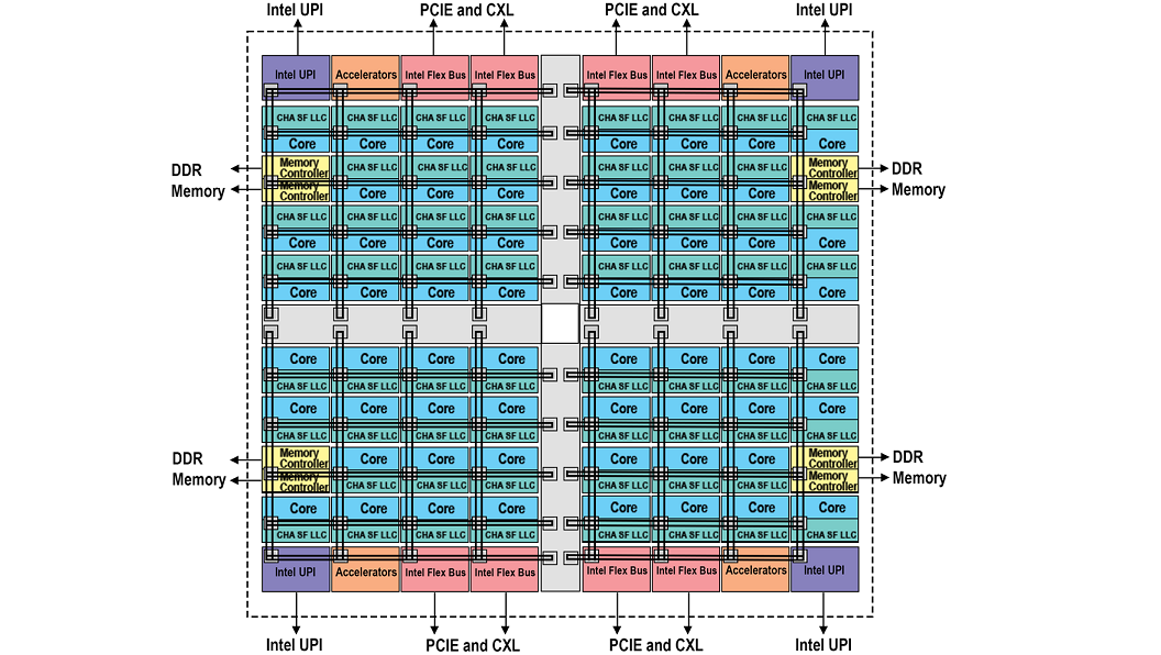
Figure 1 – Block Diagram Representing UMA
Over the course of time the density of processors, memory controllers, interconnects and supporting infrastructure continues to expand on the die, while the geometry gets smaller. This correlates to an increase in the amount of time it takes for data to move from one side of the die to another. A uniform memory access (UMA) domain is where we originally started and is still an option on the system. It provides a single contiguous address space that is interleaved among all the memory controllers. UMA does not provide a way to optimize data flow from the nearest resources. This is normally done through processor affinity which is a way to dictate what processor(s) a given software thread uses. Therefore, all cores have equal access to the last level cache and to memory when they are part of an UMA domain. In this situation you may have a processor accessing a memory controller or a slice of the last level cache that is on the opposite side of the die versus from the nearest.
Sub-NUMA Clustering
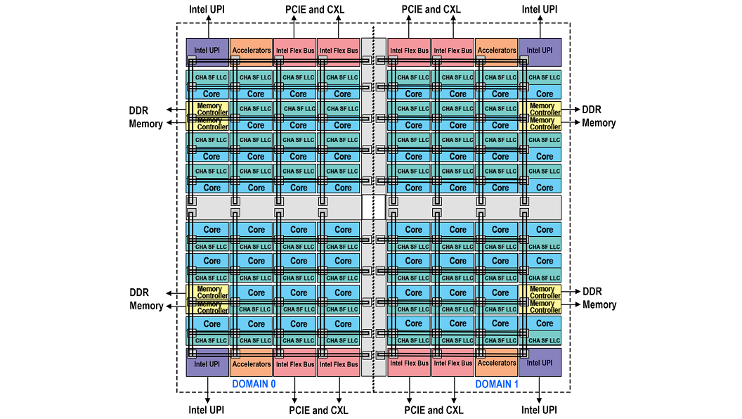
Figure 2 – Block Diagram Representing Domains Of sub-NUMA With Two Clusters
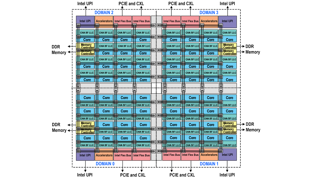
Figure 3 – Block Diagram Representing Domains Of sub-NUMA With Four Clusters
To decrease the latency of data movements across the die sub-NUMA clusters (SNC) were introduced. In a two cluster SNC (SNC-2), two localization domains exist within a processor. Each domain has mapped addresses from the local memory controller and local Last Level Cache (LLC) slices. Processors in the local domain will use the local memory controller and local LLC slices. Processors in the local domain will observe lower LLC and memory latency compared to latency on accesses mapped to locations outside of the same SNC domain.
SNC has a unique location for every address in the LLC, and it is never duplicated within the LLC banks. Localization of addresses within the LLC for each SNC domain applies only to addresses mapped to the memory controllers in the same socket. All addresses mapped to memory on remote sockets are uniformly distributed across all LLC banks independent of the SNC mode. Therefore, even in the SNC mode, the entire LLC capacity on the socket is available to each core, and the LLC capacity reported through the CPUID is not affected by the SNC mode.
Figure 2 represents a two-cluster configuration that consists of SNC Domain 0 and 1 in addition to their associated cores, LLCs, and memory controllers. Each SNC domain contains half of the processors on the socket, half of the LLC banks, and one of the memory controllers with its associated DDR channels. The affinity of cores, LLC, and memory within a domain are expressed via software using the OS NUMA affinity parameters, which can take SNC domains into account in scheduling tasks and allocating memory to a process for optimal performance.
The latest generation of silicon provides either 2 domain or 4 domain versions of SNC. SNC is enabled at the BIOS level and requires that the memory be symmetrically populated, and the software must be optimized to take advantage of it. If these criteria can be met it will provide the best performance out of all the modes of operation.
Hemisphere and Quadrant Modes
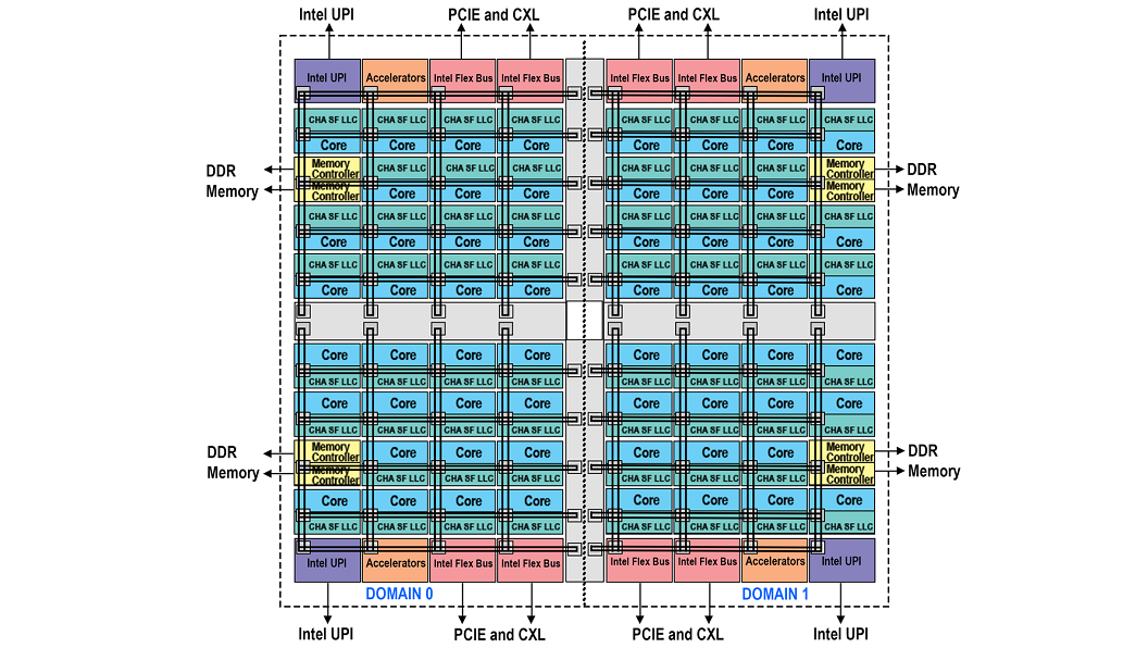
Figure 4 – Block Diagram Representing Domains Of Hemisphere Mode
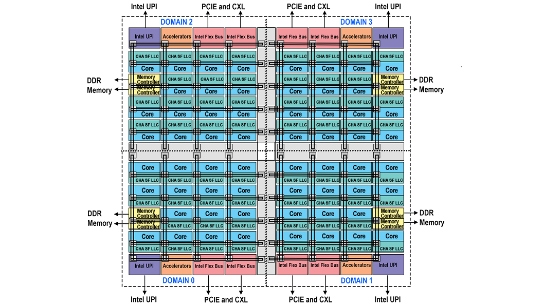
Figure 5 – Block Diagram Representing Domains Of Quadrant Mode
For those customers who can meet the requirement of having symmetrically populated memory but who do not wish to alter their software as must be done with sub-NUMA clustering there are two new modes available. Hemisphere and Quadrant divide the die into either two or four domains respectively. Each processor has access to all the caching agents and memory controllers. However, based on a hash function each home agent will automatically ensure the caching agent is routed to the closest memory controller within the same domain. Once a processor accesses a caching agent the distance is minimized as it is always going to interact with the closest memory controller. These modes of operation will tend to produce a better performance result as compared to UMA but not as good as compared to sub-NUMA clustering. The settings are found within the BIOS with Quadrant as the default. The mode used by the BIOS will be dictated by the memory symmetry. If memory symmetry cannot be met for quadrant mode, then hemisphere mode will be used. If there still isn’t enough symmetrical memory for hemisphere mode, then the system will default to UMA mode.
New Instructions
The latest generation of silicon has a new microarchitecture core that brings with it a variety of enhancements which are covered in greater detail throughout this article. In this section we will touch upon some of the instructions that are associated with these changes. A portion of the new instructions center around Accelerator interfacing Architecture (AiA). These are built into the ISA and are an enhancement on the x86 processors meant to optimize data movement by accelerator devices to host services. The instructions MOVDIR, MOVDIR64B, ENQCMD, ENQCMDS, User Interrupts, User IPIs, Umonitor, Umwait, and PAUSE are focused on the AiA operations. The MOVDIR/MOVDIR64B instructions are to offload data movements to the accelerator. The ENQCMD/ENQCMDS instructions facilitate shared and dedicated work queues allowing the hardware to manage the process. This avoids wasting a core processor resource on a persistent thread. Lastly the user interrupts, IPIs, Umonitor, Umwait, and PAUSE instructions deal with signaling and synchronization aspects of the accelerators.
Instructions to support AI workloads via Intel AMX includes Int8 for inference, Bfloat16 for inference/training, and Xsave to help with the management by the operating systems of the dedicated silicon tiles. While Intel® Advanced Vector Extensions 512 (Intel® AVX-512) includes FP16 which replicates the FP32(SP) computation instruction using a new FP16 data type to help with support for complex number arithmetic. This can be of value for signal and image processing and specifically with 5G networks.
For virtualization there is Hypervisor Linear Address Translation (HLAT) which can be used by the VMM to enforce guest linear address translation to guest physical addresses. When combined with enhanced page-table capability it helps to ensure VMM-enforced guest translations are not tampered with by untrusted system software.
On the security side Intel® Control-Flow Enforcement Technology (Intel® CET) defends the shadow stack against return-oriented programming by implementing a duplicate shadow stack that is managed by the CPU. The two stacks are compared on a call to make sure there are no unexpected discrepancies.
Lastly Intel TSX has two new commands, XSUSLDTRK (suspend tracking load address) and XRESLDTRK (resume tracking load address). These commands allow programmers to choose which memory accesses do not need to be tracked in the TSX read set. This has the potential to benefit in-memory database by reducing the capacity aborts by allowing the software to exclude certain load addresses from entering the transaction read set.
For additional information see the Intel® 64 and IA-32 Architectures Optimization Reference Manual and the Intel® Architecture Instruction Set Extensions Programming Reference.
Built-In Accelerators
In the fourth generation of the Intel Xeon Scalable processor family an emphasis has been placed on incorporating multiple accelerators into the processor package. The accelerators bring new functional capabilities to support popular use cases associated with AI, cryptographic, in-memory database analytics, and data movement operations. They also help to optimize the throughput of code simply because they are physically closer to the processor. The accelerators can work individually or in combination with each other to help create a multi-layered approach to improving performance. They include next-gen Intel® QuickAssist Technology (Intel® QAT), Intel® In-Memory Analytics Accelerator (Intel® IAA), Intel® Data Streaming Accelerator (Intel® DSA), and Intel® Advanced Matrix Extensions (Intel® AMX).
Cryptographic Acceleration
Intel has longstanding practice of enhancing cryptographic cipher performance through the introduction of new instructions, improvements to processor microarchitecture, and innovative algorithm optimizations. Intel’s latest version of Intel Xeon Scalable Processor is no exception and provides performance improvements for a variety of widely adopted public key cryptographic ciphers, symmetric ciphers, and cryptographic hash algorithms.
Public Key cryptography is a category of cryptographic ciphers widely used for authentication and key exchange when establishing a secure TLS connection between two systems. Based on large integer math, the ciphers require compute intensive multiplication and squaring primitives to support the cryptographic algorithm. The AVX512 Integer Fused Multiply Add (IFMA) VPMADD52* instructions support efficient large number multiplication operations with a four-fold increase in parallelism over previous architectures. RSA, ECDSA, and ECDHE public key cryptographic cipher performance can be improved incorporating these instructions into your specific algorithm computation primitives. When these instructions are used in combination with cryptographic multi-buffer processing techniques can yield significant performance improvements.
Advanced Encryption Standard (AES) symmetric ciphers can be optimized to take advantage of Vectorized AES-NI. When used with 512-bit wide registers, one can process up to four AES 128-bit blocks per instruction delivering a significant improvement in bulk encryption throughput in a variety of modes (Ex. AES-GCM).
Cryptographic hash algorithms benefit from the introduction of Vectorized Carryless Multiply (CLMUL) and SHA-Extensions being added to the architecture. Vectorized CLMUL provides throughput gains for processing Galois Hash (GHASH) and with specific instructions added to help support SHA-256, this aims at improving performance over previous Intel Xeon Scalable processor architectures. These new instructions are compatible with Data Plane Development KIT DPDK, Intel OpenSSL Engine, Intel Storage Acceleration library (ISAL), IPSec Multi-Buffer Library and IPP Multi-Buffer Library.
Previous generations of Intel QAT resided within the chipset. While the next generation of Intel QAT has been moved inside of the processor package optimizing its interaction with the processor cores due to physical proximity. This next generation provides 200Gbs Crypto, 160Gbs verified compression, 100kops PFS ECDHE and RSA 2K Decrypt. The technology can provide benefits of data compression for data lakes, file systems, distributed storage systems, memory infrastructure optimization, next generation firewall, wireless core and edge, content delivery controllers, OpenSSL, SSL/TLS, and more.
Intel® In-Memory Analytics Accelerator (Intel® IAA)
Big data and in-memory databases are frequently utilized together to optimize results for various use cases such as fraud prevention in financial services, personalization of products and services, as well as analysis of sensor data to look for preventative maintenance. Intel IAA is an accelerator that has been designed to help benefit in-memory databases and analytic workloads. There are three main areas that Intel IAA can assist with analytics primitives (scan, filter, etc.), sparse data compression and memory tiering.
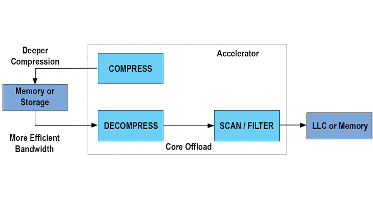
Figure 6 – Compression/Decompression
Compression and decompression are frequently used or desirable when dealing with big data stored in-memory or on a storage array. Decompression maybe a requirement as part of applying data analytics such as with a table scan. The accelerator is designed to pull data from the last level cache, memory or storage decompress it and apply analytics primitives. The output from the transaction can be sent back to the cache, memory or storage. All of this work is offloaded from the processor core.
For AI workloads there can be many zero values introduced into the matrix of data that is being worked on. These zero values are known as sparsity. If sparsity can be reduced an improvement in the performance should follow for AI workloads. The accelerator has the capability to pull data from memory and apply sparsity compression. The data is then sent to the last level cache to be worked on by the AI workload.
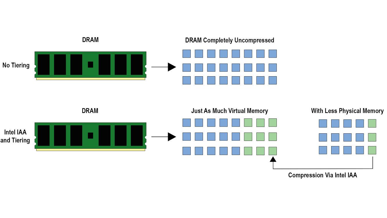
Figure 7 – Memory Tiering
Memory tiering is the concept of dividing memory into different areas to help with resource management. Hot data that is more frequently executed can reside in an area where it has a faster throughput to the processor while less used cold data can reside on an area that has slower throughput to the processor. The more frequently used memory might be stored in memory while less used data might be stored on a hard drive. Intel IAA can provide a hybrid solution for memory tiering by compressing a portion of the data within the memory space creating a warm location for the data to reside within. The memory footprint for a workload and the total cost of ownership for a data center may be reduced via compression-based memory tiering.
Intel IAA has up to four instances per socket that are available to offload data from the processor core. From a software perspective each instance is exposed as a PCI-Express complex integrated endpoint. Intel IAA supports a variety of PCI-SIG* Defined services to provide highly scalable configurations. It also supports shared virtual memory allowing the device to operate directly in the applications virtual address space without requiring pinned memory.
Intel IAA instances are identified by the operating system via the Intel® Data Accelerator Driver (IDXD) which can be utilized by software libraries and frameworks to manage work queues. One way to do this is through the Intel® Query processing Library. It can be used to assign work queues and groups to Intel IAA at which point the API can be called to offload work to the hardware accelerator. The Intel® In-Memory Analytics Accelerator (Intel® IAA) Enabling Guide covers the process for those who would like an overview of enabling Intel IAA. While deeper insight into the architecture information can be found within the Intel® In-Memory Analytics Accelerator Architecture Specification.
Intel® Data Streaming Accelerator (Intel® DSA)
Intel DSA is a replacement to Intel® Quick Data Technology. It is designed to help offload common data mover operations from the processor cores that might be found in storage applications, hypervisors, persistent memory operations, networking applications, operating system cache flushing, page zeroing and memory moves. More specific uses that Intel DSA may assist with include virtual machine fast checkpoint analysis, vSwitch network virtualization, fast replication across non-transparent bridge (NTB), and applications that focus on analytics, in-memory databases, and messaging.
From a hardware perspective Intel DSA has up to four instances per socket depending on the model, available to offload data from the processor core. It supports the data movement between any component on the platform including all compatible attached memory and IO devices. For example, the data movement between the processor cache to main memory, between the processor cache to an addon card, and between two addon cards is supported.
From a software perspective the data can be shared concurrently across the operating system, virtual machine manager, virtual machines, containers, and application processes. A shared virtual memory space allows the device to operate directly in the applications virtual address space without requiring pinned memory. Each instance of Intel DSA is exposed as a PCI-Express complex integrated endpoint and supports a variety of PCI-SIG* Defined services creating highly scalable configurations.
Intel DSA instances are identified by the operating system via the Intel® Data Accelerator Driver (IDXD) which can be utilized by software libraries and frameworks to manage work queues. Compatible libraries for ease of adoption can be found in the Data Plane Development KIT DPDK, the Storage Performance Development Kit, with a more generic dmadev abstraction that can be used with other copy-offload engines, DMA drivers, and an example application. Additional resources include: Introducing The Intel® Data Streaming Accelerator (Intel® DSA), Intel® DSA Specification, Intel® Data Accelerator Driver GitHub* repository, Intel® Data Accelerator Driver Overview on GitHub.io, Intel® Data Accelerator Control Utility and Library, Shared Virtual Memory, Intel® Scalable I/O Virtualization, Intel® 64 and IA-32 Architectures Software Developer Manuals, Intel® Data Streaming Acceleration Architecture Specification and the Intel® Data Streaming Accelerator User Guide.
Intel® Advanced Matrix Extensions (Intel® AMX)
[embed]6318295073112[/embed]
Intel® Advanced Matrix Extensions (Intel® AMX) is designed primarily to improve deep learning inference & training performance. It is a new 64-bit programming paradigm consisting of two components: a set of 2-dimensional registers (tiles) representing sub-arrays from a larger 2-dimensional memory image, and an accelerator able to operate on tiles, the first implementation is called TMUL (tile matrix multiply unit). Intel AMX provides the programmer with configurable tile sizes for flexibility supplied as metadata. A single instruction is capable of autonomously executing multi-cycles in the tile and accelerator hardware. Since execution is driven through metadata, an existing Intel AMX binary could more easily take advantage of changes over time in the Tile sizes without adjustments to the software coding.
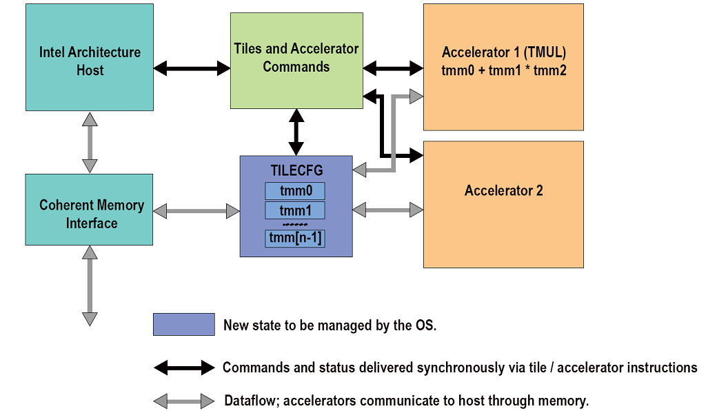
Figure 8 - Conceptual Diagram Of The Intel AMX Architecture.
An Intel architecture host drives the algorithm, the memory blocking, loop indices and pointer arithmetic. Tile loads and stores and accelerator commands are sent to multi-cycle execution units. Intel AMX instructions are synchronous in the Intel architecture instruction stream and the memory loaded and stored by the tile instructions is coherent with respect to the host’s memory accesses. There are no restrictions on interleaving of Intel architecture and Intel AMX code or restrictions on the resources the host can use in parallel with Intel AMX (e.g., Intel AVX512). There is also no architectural requirement on the Intel architecture compute capability of the Intel architecture host other than it supports 64-bit mode.
Intel AVX512 code that is using the FP32 data type will continue to use the Intel AVX512 code path on the platform. Developers that want to convert their FP32 based deep learning models over to BF16 or INT8 for use with Intel AMX can utilize the Intel® Neural Compressor. This tool will make the conversion process easier. While the following article provides you with a code sample tutorial, Code Sample: Intel® Advanced Matrix Extensions (Intel® AMX) - Intrinsics Functions and you can get code samples directly on Github.
Intel AMX supports int8 (all sign combinations) with int32 accumulation as well as Bfloat16 with IEEE SP accumulation. It is supported by various tools and libraries which include Intel® oneAPI Deep Neural Network Library (oneDNN), Intel® oneAPI Math Kernel Library (oneMKL), Intel® oneAPI Collective Communications Library (oneCCL), Intel® oneAPI Data Analytics Library (oneDAL), Intel® Neural Compressor, and Intel OpenVINO Toolkit version. More detailed information can be found in Intel® Architecture Instruction Set Extensions Programming Reference. Support for this new technology can be found in Linux Kernel version 5.18+ and Windows Server version 2022+. Use cases that may benefit from Intel AMX include Natural language processing, media analytics, media processing and delivery, image recognition, machine language translation and reinforcement learning.
Intel® Dynamic Load Balancer (Intel® DLB)
There has been an increase in the number of work queues due to the introduction of the new accelerators. Intel DLB has been provided to help manage these work queues across the processor cores using dedicated logic. The dedicated logic manages the queue head and tail pointers stored in memory that are used by the producers and consumers. The hardware frees up the software from this process improves scalability, avoids spinlock penalties, and atomicity is maintained with load variations as the work is dynamically distributed across the processor cores.
While Intel DLB can balance the loading for the accelerators it isn’t limited to just that application. Traffic generated in other areas of the platform such as from CXL or the network can also be managed. Network traffic for example can benefit from Intel DLB in the areas of streaming data processing, elephant flow handling, vSwitch, Vector Packet Processing routers, and IPSec security gateways.
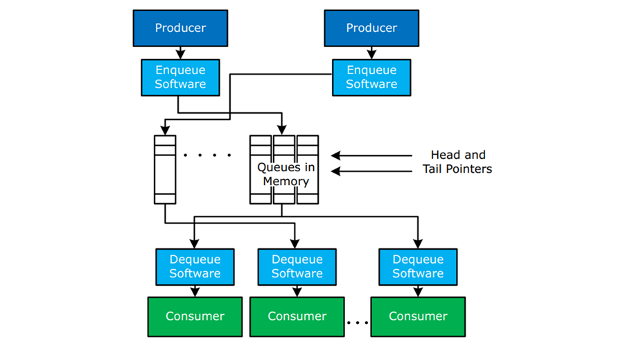
Figure 9 – Queues Managed By Software
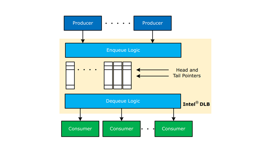
Figure 10 – Queues Managed By Dedicated Hardware Logic (Intel DLB)
The use of queues in memory with traditional method of work communication between producers (adding to the queue) and consumers (removing from the queue).
In figure 9 the queues are managed by software only (without Intel DLB).
- Queue keeps the work list in order
- Queue head/tail pointers also stored in memory and their status is verified via enqueue/dequeue software
- Fundamental performance and algorithmic limitations to this approach:
- Impact Of Lock Latency
- Lock Contention
- Memory Latency
- Cache And Snooping Behaviors
- Polling Of Multiple Queues
In figure 10 the queues are managed by Intel DLB.
- Head/tail pointers and queue are stored within Intel® DLB local memory
- Compute and polling limitations are solved by using purpose-built logics within Intel® DLB (represented by the Enqueue/Dequeue Logic blocks)
- Performance improves due these changes include:
- Core Cycles Freed To Do Other Work
- Lock-Free Access
- Polling Reduction
- No Cross-Core Snooping For Queue Access
- Reduced Impact Of Memory And Caching Behaviors
- High Queuing Throughput
- Load Balance Across Consumers
Resources:
Queue Management and Load Balancing on Intel® Architecture
Compute Express Link™ (CXL™)
Compute Express Link™ (CXL™) is an open interconnect standard that utilizes the fifth generation PCI express physical layer providing more efficient movement of user and kernel level data between the host processor and the attached devices such as Field Programmable Gate Arrays, Graphics Processor Units, or network controllers. CXL makes it possible for cache coherent accesses from the attached devices to the host processor cache. Along with memory accesses from the host processor to memory on the attached device. The built-in accelerators on the platform such as Intel IAA, Intel DSA, Intel QAT, and Intel AMX utilize CXL to optimize their productivity.
CXL has a flexible processor port attached to the PCI express bus that is capable of auto-negotiating the protocols associated with either PCI express or CXL. A device attached to PCIe has to go through layers and checks in order for the data to reach the processor. While a device using the CXL protocols is able to bypass the PCIe hierarchy and obtain a more direct communication with the processor through address translation and access to the physical address space. This means that by comparison CXL is able to provide increased bandwidth and lower latencies as compared to PCI express.
On our latest generation of the platform, we have what is called a flex bus. The flex bus is capable of providing both standard PCIe interconnects as well as up to four CXL interconnects 16 lanes wide with up to 32 Gigabits per second. The flex bus supports hot swappable PCIe devices, while CXL devices are only recognized and supported by the BIOS at boot time.
There are three protocols utilized by CXL. They are CXL.io, CXL.cache, and CXL.mem.
CXL.io protocol operates in similar to the PCIe protocol and follows the same base PCIe specifications for the transaction and link layers. It is used for load and store operations, discovery, interrupts, enumeration, RAS features, etc. Regardless of the use case CXL.io is a required protocol in order to manage and operate the CXL device. CXL.io does provide some additional enhancements that are specific to the CXL protocol for management of the device, memory address translation services and power events.
CXL.cache is a protocol that utilizes hardware cache coherency with a 64 byte cache line. It is designed to provide coherent access from the attached device to the processor cache. The protocol will snoop the coherent cached state for the attached device that made the request. It is possible to use a subset of transactions to avoid snoop requests if the attached device doesn’t implement a cache. The protocol uses host physical addressing only and most of the requests are unordered.
CXL.mem protocol provides a host processor with ability to perform simple reads and writes to an attached device that has its own private memory. The protocol is transactional which allows it to interface with any type of memory. Therefore, you can use DDR, Optane, or even HBM and it could be in a flat model, far memory or even a mix of near and far memory. The protocol uses host physical addressing only.
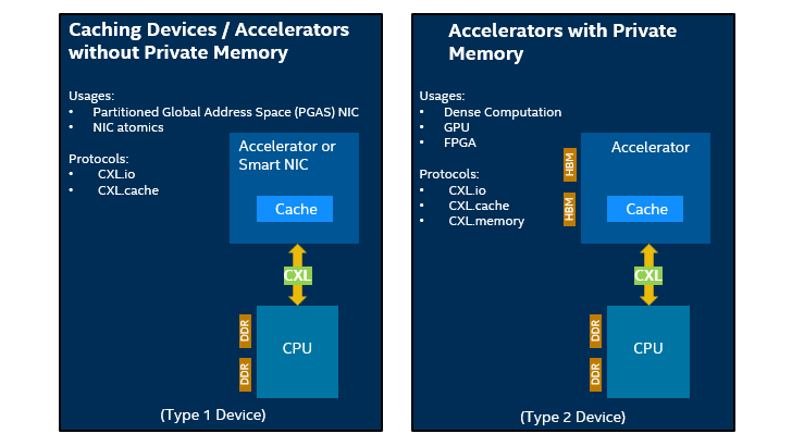
Figure 11 - Use Case Examples
The platform supports CXL version 1.1 with two different use models. Type one use model is associated with attached caching devices without private memory while type two use model is associated with an attached device with private memory.
Type one devices might include a smart NIC or an accelerator. The CXL.io protocol can be used to communicate and configure the devices. While the CXL.cache protocol can be used for non-coherent flows to read the latest value of the cache. Alternatively, the entire cache line can be updated without taking ownership by the attached device using push write flows. The CXL.cache protocol can also use coherent flows to take ownership of the cache line to modify it.
Two of the more interesting use cases associated with Type one devices would be PGAS NICs and NIC atomics. Partitioned Global Address Space (PGAS) programming models offer a shared address space model that simplifies programming while exposing data and thread locality to enhance performance. Normally this model uses PCIe that must deal with PCIe’s ordering scheme, which in this situation can require a serialized approach. CXL takes the PGAS model utilized by the NICs into a much more simplified and faster solution primarily because it is able to bypass the PCIe ordering scheme. It is able to do this by prefetching the cache locations and then ordering transactions. The second use case can benefit NICs that support different atomic types. PCI express protocols can limit which atomics end up being useable by the NIC as it typically requires industry acceptance. CXL.cache however doesn’t have the same atomic limitations found with PCI express protocols because you can directly access them within the cache. This opens up the possibility for atomics associated with floating point operations used by NICs on the CXL bus.
Type two devices are when the processor is working with other accelerators that have memory attached. This could include other processors, graphics processing units or field programmable array units. The attached memory on any of these devices appears as additional system memory to the host processor but with a different proximity and latency. The software can determine the proximity and latency for the attached device memory and access it via the CXL.mem protocol. This use case may benefit In-memory databases and AI deep learning applications.
From a programming perspective legacy software that was designed to interact with PCIe devices will view CXL devices as part of a PCIe compliant root complex integrated endpoint. The devices will be capable of standard PCIe interactions via software including multi-function and SR-IOV. In terms of software designed to operate with CXL it starts with the firmware. The firmware will initialize the bus, setup the registers, and communicate the address to the operating system using the CXL early discovery table which is a new type of an ACPI table. By following the CXL 1.1 specification and utilizing the CXL Device Designated Vendor Specific Extended Capability (DVSEC) structure the programmer can create software to interact with the CXL device.
Resources:
CXL Memory Device Software Guide describes how system firmware, OS and UEFI may configure CXL Type 3 devices, much of the information will be applicable to CXL 1.1
CXL-cache/mem Protocol Interface (CPI) specification has been developed to map coherent protocols between an agent and a fabric
Streaming Fabric Interface (SFI) Specification has been developed to map Load/Store protocols (like PCIe) between an agent and a fabric.
Intel® Scalable I/O Virtualization (Intel® Scalable IOV)
Scalability is a necessity as the capabilities of the processor and platform continue to expand over time. Intel Scalable IOV is designed to handle the increased demand for IO operations associated with virtualized environments. Intel Scalable IOV has replaced the pre-existing Single root IO virtualization (SR-IOV) technology by providing a flexible composition of Virtual Functions using software from native hardware interfaces. While SR-IOV implements a complete virtual function interface, Intel Scalable IOV instead uses a lightweight assignable device interface (ADIs) that is optimized for fast data path operations for direct access from the guest. Intel Scalable IOV easily interfaces with PCIe or CXL via Process Address Space IDs (PASIDs). Thereby allowing multiple guest operating systems to natively share PCIe or CXL devices simultaneously. Intel Scalable IOV supports all the accelerators found on the latest generation of silicon as well as any discrete accelerators.
Virtual devices are dynamically composed from fast-path resources and slow-path software emulation, therefore the technology requires support by the operating system and virtual machine manager through device drivers and firmware. For additional insights see the Intel® Scalable I/O Virtualization Technical Specification.
Additional Resources:
Technical Overview Of The Intel® Xeon® Scalable processor Max Series
Intel® In-Memory Analytics Accelerator (Intel® IAA) Enabling Guide
Proof Points of Intel® Dynamic Load Balancer (Intel® DLB)
Code Sample: Intel® Advanced Matrix Extensions (Intel® AMX) - Intrinsics Functions
Intel® Data Center GPU Max Series Technical Overview
Intel® Performance Counter Monitor (Intel® PCM)
The Author: David Mulnix is a software engineer and has been with Intel Corporation for over 20 years. His areas of focus include technical content development and training, software automation, server performance and power analysis with SPECPower, and he supported the development effort for the Server Efficiency Rating ToolTM.
Contributors: Arijit Biswas, Ruchira Sasanka, Vinodh Gopal, Wajdi Feghali, Mahesh Wagh, Alberto Villarreal and Dan Zimmerman
Notices/Disclaimers
Performance varies by use, configuration and other factors. Learn more on the Performance Index site.
No product or component can be absolutely secure.
Code names are used by Intel to identify products, technologies, or services that are in development and not publicly available. These are not "commercial" names and not intended to function as trademarks
Intel disclaims all express and implied warranties, including without limitation, the implied warranties of merchantability, fitness for a particular purpose, and non-infringement, as well as any warranty arising from course of performance, course of dealing, or usage in trade
Your costs and results may vary.
Intel technologies may require enabled hardware, software or service activation.
© Intel Corporation. Intel, the Intel logo, and other Intel marks are trademarks of Intel Corporation or its subsidiaries. Other names and brands may be claimed as the property of others.