Overview
This tutorial shows you how to use the Qsys* system integration tool to create a custom Field Programmable Gate Array (FPGA) hardware design using IP available in the Intel® FPGA IP library. Qsys speeds embedded system design by creating a configurable interconnect between IP blocks. Developers who create their own IP blocks can publish them to the Qsys IP library for reuse in their systems. After completing this tutorial, you will have a system design like the one shown in the block diagram below:

Level: beginner
Materials
Hardware
Windows* or Linux* development host PC
Software
The following are required:
Installed Intel® Quartus® Prime Design Software. Either the Quartus® Prime Lite Edition Software or Quartus® Prime Standard Edition Software, but not the Intel® Quartus® Prime Pro Edition Software. This was accomplished in the Program Your First FPGA Device tutorial.
A completed Intel® Quartus® software project from the Program Your First FPGA Device tutorial. If you have not completed that tutorial you can:
- Click here to complete the Program Your First FPGA Device tutorial.
- Click here to download a zip file which contains the completed project files from the Program Your First FPGA Device tutorial. Unzip the files to a unique project folder on your PC.
Where Should I put Project Files?
Here are a few guidelines you should adopt when choosing a directory for your project:
- Don't put projects within the Intel® Quartus® tool directory. New Intel Quartus versions come out every six months, so placing them within a specific version directory will make them 'orphans' once a new version is installed. Even worse, you might lose them if you delete the older tool version.
- Avoid paths with spaces in the name since some of the tools don't like spaces in directory paths.
- Use directories where you have read/write access. This sounds intuitive, but sometimes IT departments limit administrator rights. Be sure the folder you create doesn't require admin rights.
Note: User experience may vary when using earlier or later versions of Intel® Quartus® Prime Software Suite. Screenshots in this document are based on the 17.0 release.
Create the Qsys* System
This section describes the steps required to create a Qsys system. It assumes that you have the completed blink project from the Program Your First FPGA Device tutorial open in the Intel Quartus development software.
1. Launch the Intel Quartus software, click Open Project from the File menu, and select the blink project from the previous tutorial (blink.qpf).
2. Launch Qsys by clicking the Qsys button on the toolbar, or selecting Qsys from the Tools menu.
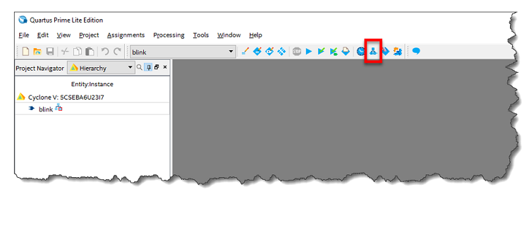
Figure 1. Qsys Button on Intel® Quartus® Prime Software Toolbar
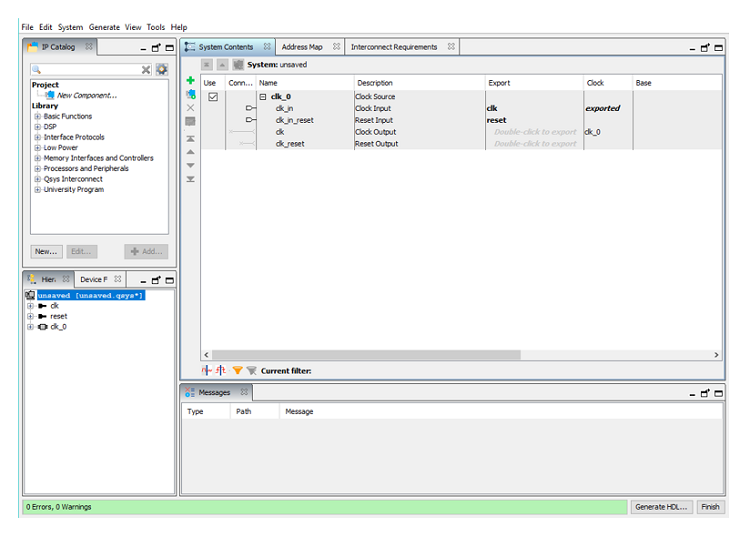
Figure 2. New Empty Qsys System
3. Qsys opens to an unsaved system, with one clock source component already instantiated. To add another IP block, use the IP Catalog pane in the left-hand column. In the search bar, start typing 'on-chip memory' until you see the On-Chip Memory (RAM or ROM) IP appear.
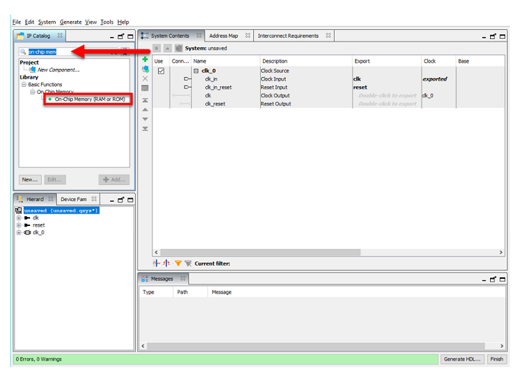
Figure 3. Search for On-Chip Memory Component
Add On-Chip Memories
1. Double click on the On-Chip Memory component (or select it with the mouse and click the Add… button) to insert a new instance into the system. This opens the parameter dialog for the On-Chip Memory IP. Change the Slave S1 Data Width to 64, and change the Total Memory Size field to 65536 to make this a 64-kilobyte on-chip memory that supports 64-bit accesses, then click the Finish button at the bottom of the dialog box.
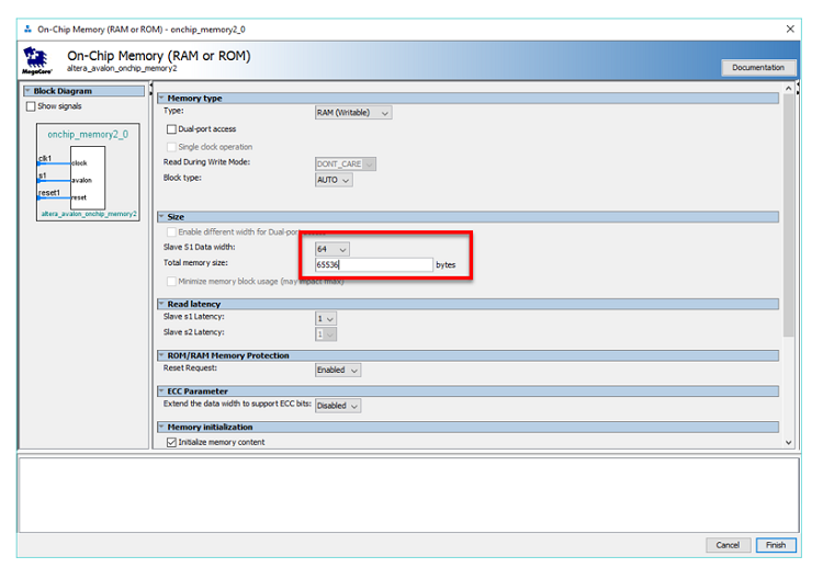
Figure 4. On-Chip Memory Parameters Dialog
2. With the new memory component instantiated in the system, we should give it a more meaningful name. To rename components in Qsys, select the component then right click to bring up the context pop-up menu, and select Rename. Rename the on-chip memory from onchip_memory2_0 to oncram_64k.
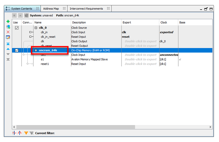
Figure 5. Renamed On-Chip Memory Component
3. To connect components in Qsys, use the Connections column in the System Contents pane. Possible connections of similar types are presented as circles at the intersection points and shaded in gray. Click the circle associated with the ocram_64k clk1 and reset1 signals to connect them to the clock and reset sources.
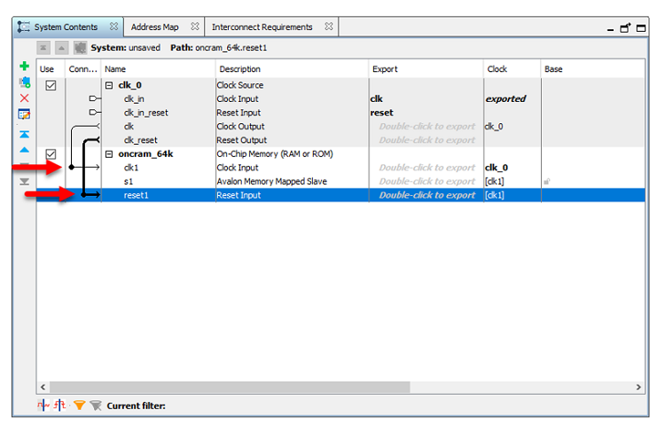
Figure 6. Clock and Reset Connections to On-Chip Memory
Notice how the Avalon Memory Mapped Slave connection on the on-chip RAM (S1) does not yet have an available connection. That connection will not appear until an IP with an Avalon Memory Mapped Master is added, which will be done in a later step.
Also, note that hovering the mouse over a connection point brings up a tooltip that details the interfaces to be connected. This can be useful while building larger systems.
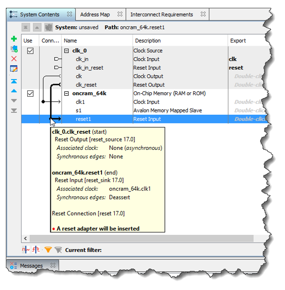
Figure 7. Connection Point Tooltip Pop-ups
Adding other IP cores follows the same process. To complete the system, add the following IP cores, and connect the clock and reset interfaces for each.
4. Add a second, small On-Chip Memory (RAM or ROM), with 32-bit data width and 16-byte memory size. The importance of this seemingly redundant component will be explained in a later step. Rename this component to default_16b.
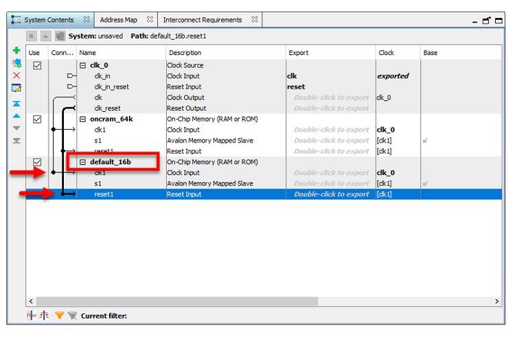
Figure 8. default_16b On-Chip Memory Component
Add Parallel I/O
1. Add a PIO (Parallel I/O) component with an 8-bit output only. Rename this component to led_pio.
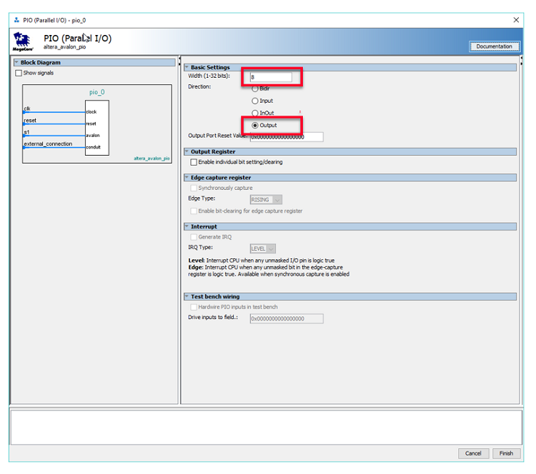
Figure 9. PIO Component Parameters Dialog
2. Export the external_connection interfaces as led_pio by double clicking next to the external_connection interface in the Export column and then edit the Export name to read led_pio.
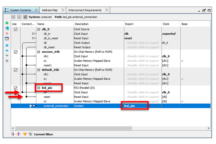
Figure 10. PIO: Export External Connection as led_pio
3. Add a PIO component with a 1-bit input only. Rename this component to button_pio and export the external_connection interface as button_pio.
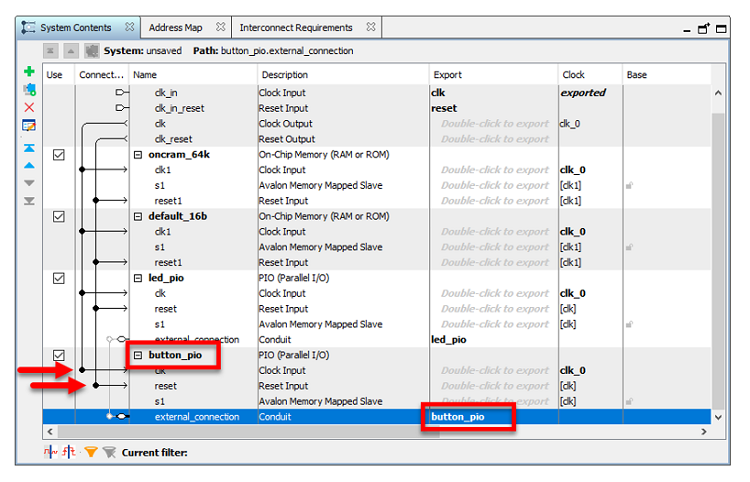
Figure 11. PIO: Add 1-bit Input button_pio
4. Add a PIO component with a 4-bit input only. Rename this component to switch_pio and export the external_connection interface as switch_pio.
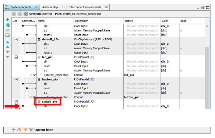
Figure 12. PIO: Add 4-bit Input switch_pio
Add a System ID Peripheral
1. Add a System ID component and assign a recognizable system ID value (type 'System ID' in the IP Catalog search bar to find it). Enter 0xde10de10 as the ID value.
What is the Purpose of the System ID Peripheral?
The System ID peripheral is a simple read-only IP core that provides Qsys systems with a unique identifier. Qsys systems containing CPUs, such as the Nios® II processor, use the system ID core to verify that an executable program was compiled targeting the actual hardware image configured in the target FPGA. If the expected ID in the executable does not match the system ID core in the FPGA, it is possible that the software will not execute correctly, and the processor can take the appropriate action (e.g. print a warning message and stop).
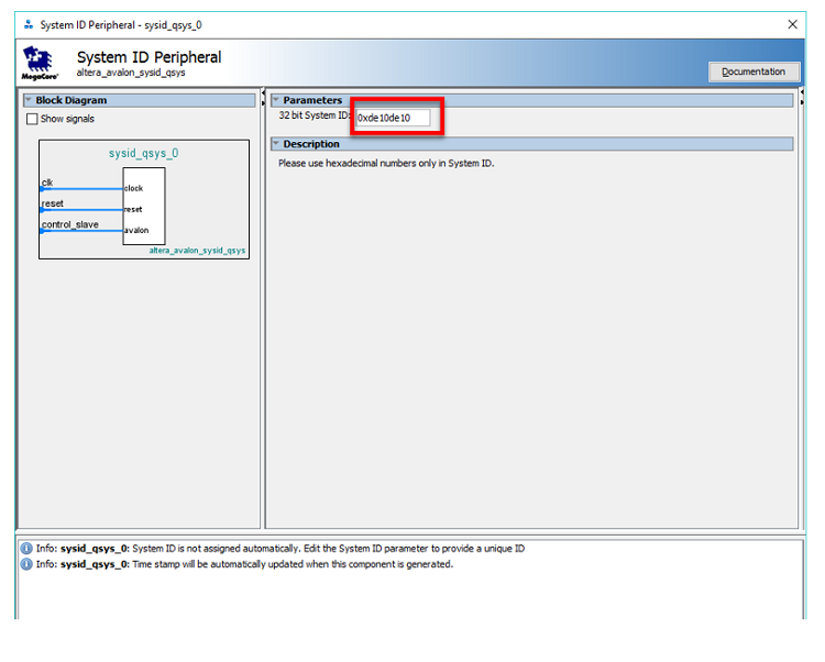
Figure 13. System ID Parameters Dialog
2. Rename this component to system_id.

Figure 14. System ID: Rename and Connect
Add a JTAG Master
1. Add a JTAG to Avalon Master Bridge. Keep the default instance name master_0.
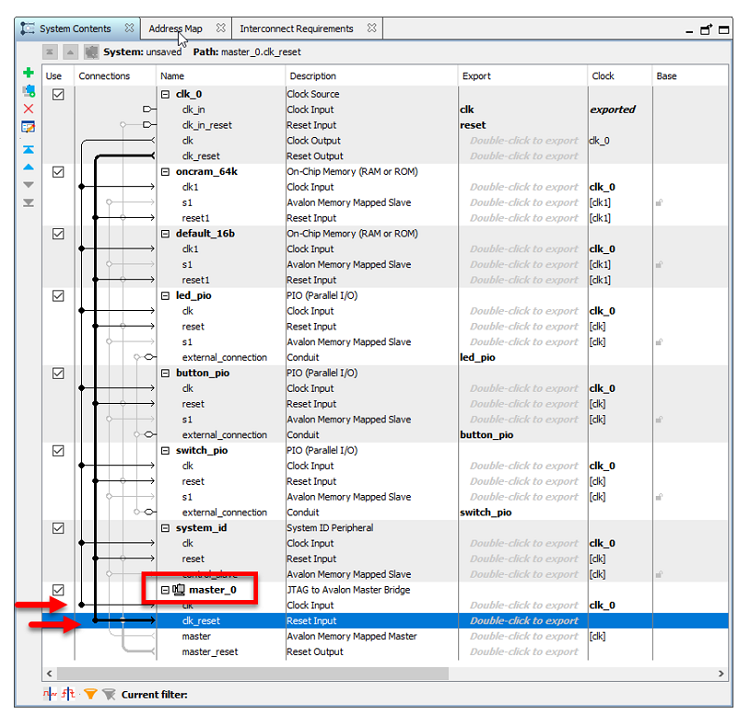
Figure 15. JTAG Master Added to System
2. Make sure the clocks and resets for all the peripherals are connected.
3. The JTAG bridge provides an Avalon master, and Qsys identifies the similar interfaces and presents the possible connections. Connect the JTAG bridge master to the Avalon Memory Mapped Slave ports of the other peripherals.
4. Connect the master_0 Reset Output to the Reset Input ports of the other IP blocks.
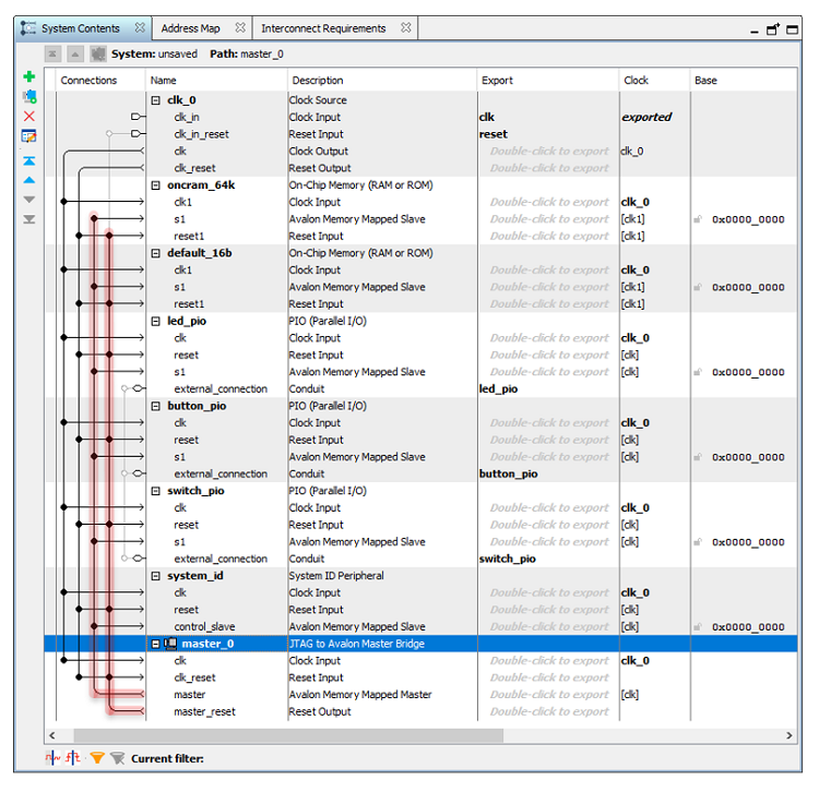
Figure 16. Fully Connected System
Assign Base Addresses
Qsys adds a preliminary address span to each slave, but initially they overlap, creating errors in the Messages pane.
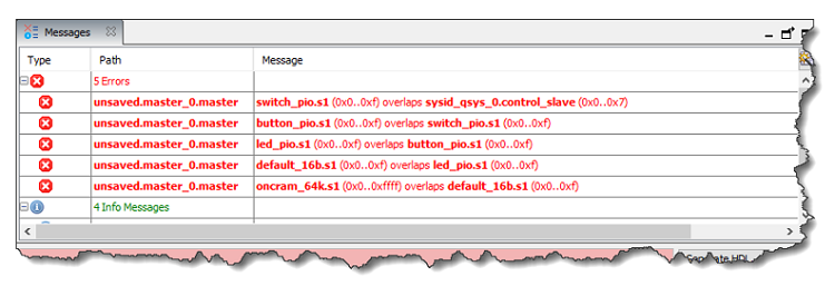
Figure 17. Address Span Overlap Errors
Resolve the address span overlap errors by:
1. Lock the ocram_64k On-Chip Memory address range to start at 0x0000_0000 by clicking the lock icon next to the address in the Base column.
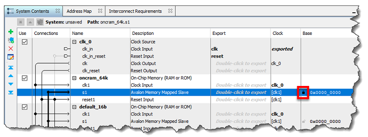
Figure 18. Lock base address of ocram_64k
2. Click the System menu, and choose Assign Base Addresses. Observe the new base addresses for all the IP blocks, and that the address for the On-Chip memory did not change.
In general, Assign Base Addresses will create the most compact address map by packing all the peripherals in order from largest address span to smallest address span. There is no guarantee that generated addresses will remain constant over multiple invocations of the Assign Base Addresses command, however locked address spans are not adjusted by the Assign Base Addresses command. For the simplicity of later tutorials, ensure the base address for each IP matches the below image; they can be edited by double-clicking the address itself.
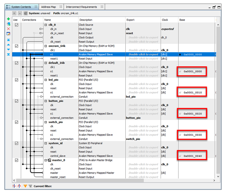
Figure 19. Properly Addressed System
3. Right-click on one of the column names in the System Contents view, and choose the Show Default Slave Column option. Scroll to the right, and check the Default Slave box for the default_16b on-chip memory.
What is a “default Slave” and why do I Need one?
Default slaves are an important concept. If a memory mapped read or write transaction is initiated to an unmapped address span, Qsys will route it to the default slave for that master in that interconnect zone. If you do not specify a default slave, then Qsys chooses by default the peripheral with the largest available address span on that interconnect. In most cases, this will be some form of memory since those are typically the largest address span peripherals in a system.
Choosing a default slave allows the designer to explicitly state that all unmapped address accesses should go to that slave. In this example tutorial, these accesses will be routed to a tiny on-chip memory that is not used for anything else, removing the possibility that data in the main memory or any other peripheral could be corrupted and allowing the designer a space to check whether errant accesses are occurring.
That default slave can be parameterized with a variety of responses to errant accesses, such as:
- Never responding (which essentially holds the master in an infinite wait request)
- Replying with a specific data pattern
- Generating an Avalon error response
- Generating an interrupt
- Generating a reset
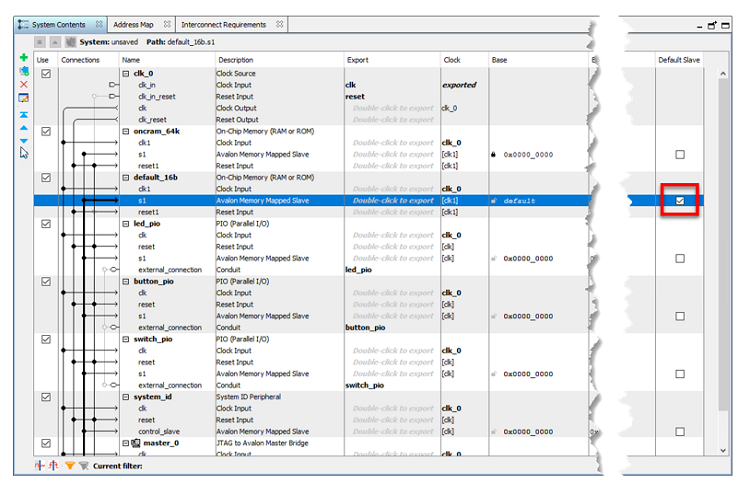
Figure 20. Default Slave Assigned to default_16b
Generate the Hardware
1. The Qsys system is complete, and now it is time to integrate it back into the Intel Quartus software project. From the File menu, select Save and use the name soc_system.qsys.
2. Close the save window when the save completes. Then, from the Generate menu, choose Generate HDL... This brings up the Generate window, uncheck the Create block symbol file (.bsf) box and click the Generate button.
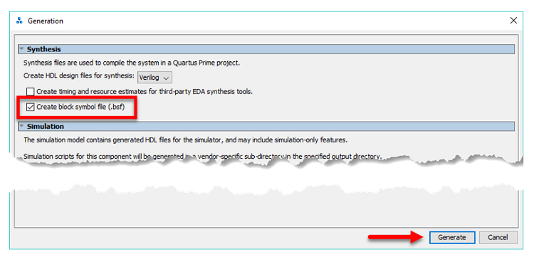
Figure 21. Qsys Generate Dialog
3. Qsys will now generate the HDL files for the IP and interconnect. Once it finishes, click the Close button, and then click the Finish button at the bottom right of the Qsys window. This will close Qsys, and present instructions to add the .qip file to the Intel Quartus software project.
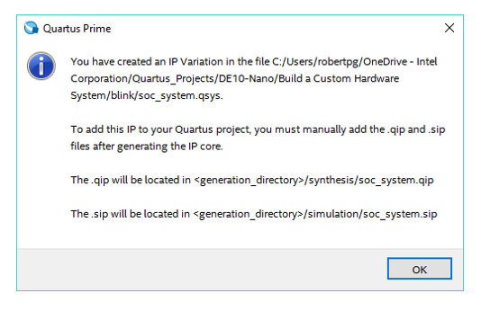
Figure 22. QIP Instruction Dialog
Integrate the Qsys* System into the Intel Quartus Software Project
This section describes how to incorporate the newly generated Qsys output into the existing blink project.
1. From the Assignments menu, choose Settings to bring up the Settings window.
2. Select Files on the left Category list. Click the ... button to the right of the File Name box to browse for the file.
3. Navigate to the .qip file using the path described in the dialog when you closed Qsys (see Figure 22).
4. Select the .qip file and click the Open button to add the file to the project.
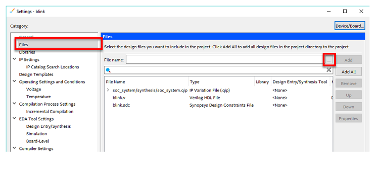
Figure 23. Adding QIP File to Intel® Quartus® Software Project
5. Click the Apply button, and then click the Ok button to close the settings window. Qsys creates an instantiation template file for the generated system, in this case it is called soc_system_ inst.v in the soc_system folder that is now in the blink project folder. It is convenient to use this to correctly instantiate the Qsys-generated system in the top-level HDL file.
6. Click the Project Navigator pull down and select Files.
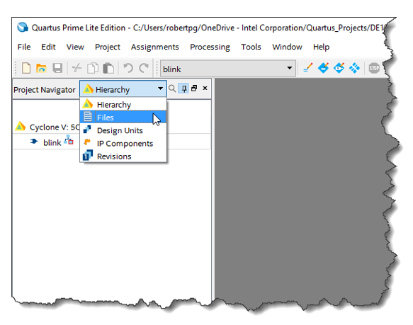
Figure 24. View Project Files
7. Open the file blink.v by double-clicking the file name.
8. Replace the existing code in blink.v with the code below:
//
// Copyright (c) 2017 Intel Corporation
//
// Permission is hereby granted, free of charge, to any person obtaining a copy
// of this software and associated documentation files (the "Software"), to
// deal in the Software without restriction, including without limitation the
// rights to use, copy, modify, merge, publish, distribute, sublicense, and/or
// sell copies of the Software, and to permit persons to whom the Software is
// furnished to do so, subject to the following conditions:
//
// The above copyright notice and this permission notice shall be included in
// all copies or substantial portions of the Software.
//
// THE SOFTWARE IS PROVIDED "AS IS", WITHOUT WARRANTY OF ANY KIND, EXPRESS OR
// IMPLIED, INCLUDING BUT NOT LIMITED TO THE WARRANTIES OF MERCHANTABILITY,
// FITNESS FOR A PARTICULAR PURPOSE AND NONINFRINGEMENT. IN NO EVENT SHALL THE
// AUTHORS OR COPYRIGHT HOLDERS BE LIABLE FOR ANY CLAIM, DAMAGES OR OTHER
// LIABILITY, WHETHER IN AN ACTION OF CONTRACT, TORT OR OTHERWISE, ARISING
// FROM, OUT OF OR IN CONNECTION WITH THE SOFTWARE OR THE USE OR OTHER DEALINGS
// IN THE SOFTWARE.
//

// create module
module blink(
        input   clk,                    // 50MHz FPGA input clock
        input   [1:0] push_button,      // KEY[1:0]
        input   [3:0] switch,           // SW[3:0]
        output  [7:0] leds              // LED[7:0]
);

// Create a power on reset pulse for clean system reset on entry into user mode
// We create this with the altera_std_synchronizer core
wire sync_dout;
altera_std_synchronizer #(
        .depth (20)
) power_on_reset_std_sync_inst (
        .clk     (clk),
        .reset_n (1'b1),
        .din     (1'b1),
        .dout    (sync_dout)
);

// Create a qsys system reset signal that is the logical AND of the power on
// reset pulse and the KEY[0] push button
wire qsys_system_reset;
assign qsys_system_reset = sync_dout & push_button[0];

/*

Qsys system instantiation template from soc_system/soc_system_inst.v:

soc_system u0 (
    .button_pio_export (<connected-to-button_pio_export>), // button_pio.export
    .clk_clk           (<connected-to-clk_clk>),           // clk.clk
    .led_pio_export    (<connected-to-led_pio_export>),    // led_pio.export
    .reset_reset_n     (<connected-to-reset_reset_n>),     // reset.reset_n
    .switch_pio_export (<connected-to-switch_pio_export>)  // switch_pio.export
);

 */

soc_system u0 (
        .button_pio_export (push_button[1]),     // button_pio.export
        .clk_clk           (clk),                // clk.clk
        .led_pio_export    (leds),               // led_pio.export
        .reset_reset_n     (qsys_system_reset),  // reset.reset_n
        .switch_pio_export (switch)              // switch_pio.export
);

endmodule

Figure 25. Copy and Paste the New Code into the blink.v File Replacing the Previous Contents
What is the Purpose of the Synchronizer in this Design?
When power is applied to the system the FPGA is configured from an external flash device and then put into 'user' mode. When the FPGA is released from configuration mode into user mode it is done asynchronously, which can violate design timing constraints and lead to design instability. The synchronizer core provides a brief and stable reset pulse that is synchronously released, allowing the design to cleanly enter operation after the FPGA is configured. If you are interested in seeing a Qsys component that can provide the power on reset functionality, checkout the power_on_reset component available in this public Git repository:
9. Click the Start Analysis & Elaboration button on the toolbar to have the Intel Quartus software process the new HDL. Select Yes when asked if you want to save your changes.

Figure 26. Start Analysis and Elaboration Button on the Intel® Quartus® Software Toolbar
There will be many more messages as the Intel Quartus software processes the Qsys-generated system. This process will identify any errors in the HDL source files or how they are configured in the project, as well as inform the Intel Quartus software of the new top-level ports that we declared in our top module.
10. The new top-level module declares many more inputs and outputs than the original design (e.g. led_pio, button_pio, etc.), so new pin constraints will need to be assigned to those inputs and outputs and the stale pin constraints can be removed. The Terasic DE10-Nano user manual contains the diagrams and schematics where these pin assignments are derived from.
From the Assignments menu, open the Pin Planner tool. Delete the stale pin (LED) by right-clicking the Node Name, selecting Edit, and pressing, then Delete.
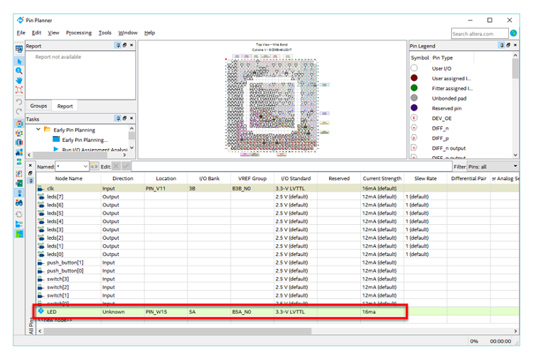
Figure 27. Pin Assignments in Pin Planner: Delete LED pin from previous design
11. Assign the new pins as in the following image. The important columns to match to the image are Location, I/O Standard, Current Strength, and Slew Rate.
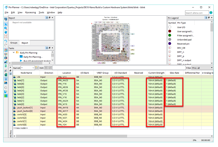
Figure 28. Pin Assignments in Pin Planner
12. Close the pin planner.
Update the Timing Constraints
1. Update the timing constraints in blink.sdc to match the newly declared ports by replacing the contents of blink.sdc with the below code. Open the blink.sdc file by double-clicking on it.
What is an SDF File, and Why do I Need One?
SDC stands for Synopsys Design Constraints and is an industry standard format which defines the timing constraints for a hardware (silicon) design such as the target frequency of the device, and the timing to external peripherals. The SDC file provides a way for Intel Quartus to verify that the system generated meets its timing requirements.
During synthesis of your FPGA, a design tool called TimeQuest Timing Analyzer* is called by Intel Quartus which reads the timing constraints files, calculates the timing of the internal FPGA signals, and compare these timings to the timing requirements specified by the SDC files. A report is created which verifies timing is met and / or identifies signals which fail to meet timing and require optimization.
2. Replace the existing code in blink.sdf with the code below:
#
# Copyright (c) 2017 Intel Corporation
#
# Permission is hereby granted, free of charge, to any person obtaining a copy
# of this software and associated documentation files (the "Software"), to
# deal in the Software without restriction, including without limitation the
# rights to use, copy, modify, merge, publish, distribute, sublicense, and/or
# sell copies of the Software, and to permit persons to whom the Software is
# furnished to do so, subject to the following conditions:
#
# The above copyright notice and this permission notice shall be included in
# all copies or substantial portions of the Software.
#
# THE SOFTWARE IS PROVIDED "AS IS", WITHOUT WARRANTY OF ANY KIND, EXPRESS OR
# IMPLIED, INCLUDING BUT NOT LIMITED TO THE WARRANTIES OF MERCHANTABILITY,
# FITNESS FOR A PARTICULAR PURPOSE AND NONINFRINGEMENT. IN NO EVENT SHALL THE
# AUTHORS OR COPYRIGHT HOLDERS BE LIABLE FOR ANY CLAIM, DAMAGES OR OTHER
# LIABILITY, WHETHER IN AN ACTION OF CONTRACT, TORT OR OTHERWISE, ARISING
# FROM, OUT OF OR IN CONNECTION WITH THE SOFTWARE OR THE USE OR OTHER DEALINGS
# IN THE SOFTWARE.
#

# inform quartus that the clk port brings a 50MHz clock into our design so
# that timing closure on our design can be analyzed

create_clock -name clk -period "50MHz" [get_ports clk]
derive_clock_uncertainty

# inform quartus that the PIO inputs and outputs have no critical timing
# requirements.  These signals are driving LEDs and reading discrete push button
# and switch inputs, there are no timing relationships that are critical for any
# of this

set_false_path -from [get_ports {switch[0]}] -to *
set_false_path -from [get_ports {switch[1]}] -to *
set_false_path -from [get_ports {switch[2]}] -to *
set_false_path -from [get_ports {switch[3]}] -to *
set_false_path -from * -to [get_ports {leds[0]}]
set_false_path -from * -to [get_ports {leds[1]}]
set_false_path -from * -to [get_ports {leds[2]}]
set_false_path -from * -to [get_ports {leds[3]}]
set_false_path -from * -to [get_ports {leds[4]}]
set_false_path -from * -to [get_ports {leds[5]}]
set_false_path -from * -to [get_ports {leds[6]}]
set_false_path -from * -to [get_ports {leds[7]}]
set_false_path -from [get_ports {push_button[0]}] -to *
set_false_path -from [get_ports {push_button[1]}] -to *

# Define timing constraints for the JTAG IO pins so that Quartus properly closes
# timing on these signal paths.  Otherwise we could have unreliable JTAG
# communication with the device over the USB Blaser II connection.
# NOTE: the 'altera_reserved_tck' clock is automatically defined by Quartus

set_input_delay  -clock altera_reserved_tck -clock_fall 3 [get_ports {altera_reserved_tdi}]
set_input_delay  -clock altera_reserved_tck -clock_fall 3 [get_ports {altera_reserved_tms}]
set_output_delay -clock altera_reserved_tck             3 [get_ports {altera_reserved_tdo}]
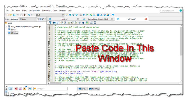
Figure 29. Copy and Paste the New Code into the blink.sdf File Replacing the Previous Contents
3. Click the Start Compilation button in the top toolbar to compile the entire design. Select Yes when asked if you want to save your changes.
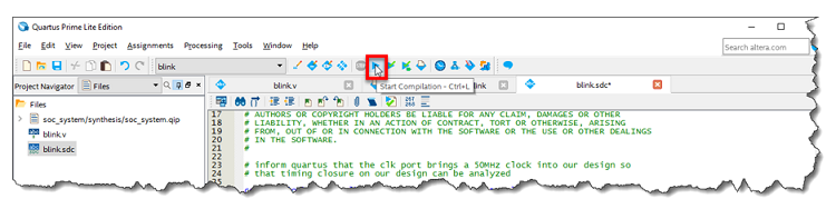
Figure 30. Start Compilation Button on Toolbar
Generate the Header Files
After your design has successfully compiled, we will perform one last activity to prepare for the next tutorial that will make use of this system on the Terasic DE10-Nano board. Since we have defined a memory mapped embedded system in Qsys with a JTAG master connected to several slave peripherals, it will be necessary for us to know what the base addresses are of the slave peripherals so we can interact with them, performing read and write transactions. That base address information is captured in Qsys. You can visualize them in Qsys several ways, but they are not convenient for software developers or other users of this system who write code for it.
Each time you generate a Qsys system, Qsys outputs a database file called <your-system-name>.sopcinfo. The Intel Quartus software provides a utility that can translate the SOPCINFO database information into a usable macro format that can be used for various purposes called sopc-create-header-files. The default functionality of sopc-create-header-files is to create C style header macros from each masters' perspective in the Qsys system. We will perform this operation in the TCL Console which is in the lower middle of the default Intel Quartus software GUI.
1. If you do not see the TCL Console pane, you can open it by selecting the View > Utility Windows > TCL Console menu.
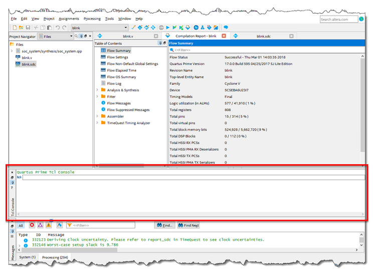
Figure 31. Intel® Quartus® Software Prime TCL Console
We will first create a directory to output the header files into, then we will create the default header file output using sopc-create-header-files and finally we will extract the base address entries out of the JTAG master header file for the FPGA peripherals that it is connected to. Copy and paste the following text into the tcl console:
# make a directory called ’qsys_headers’ to store the header files
file mkdir qsys_headers

# create a TCL variable SCHF_PATH to hold the path to the executable program
# sopc-create-header-files on your host PC using the environment variables
# provided by Quartus.
set SCHF_PATH [glob -join $quartus(quartus_rootpath) sopc_builder bin sopc-create-header-files]

# create a TCL variable BAT_PATH to hold the path to the Nios II Command Shell
# batch file on Windows platforms. The following code sequence will work on
# either Windows or Linux. For linux this variable will just be set to NULL.
set BAT_PATH {}
if {$tcl_platform(platform) == "windows"} {
set BAT_PATH [glob -join $quartus(quartus_rootpath) .. nios2eds {Nios II Command Shell.bat}]
}

# execute sopc-create-header-files to generate the header files
eval exec -ignorestderr ${BAT_PATH} ${SCHF_PATH} soc_system.sopcinfo --output-dir qsys_headers

# read the header file for master_0 into a TCL variable
set master_0_header [read [open [glob -join qsys_headers master_0.h] r]]

# output the C macro lines for the FPGA peripheral base addresses
foreach line [split ${master_0_header} "\n"] { \
if {[string  match  "*_BASE*"  ${line}]}  {puts ${line}}}
#
If you have put your Qsys system together properly and executed the above commands correctly, you should see the following output in the TCL console representing the base address definitions for the five Qsys peripherals in the FPGA fabric connected to master_0, the JTAG master bridge component.
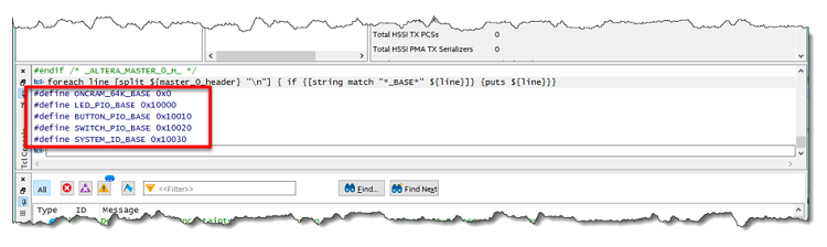
Figure 32. Base Addresses Shown in Tcl Window
That's it! You have designed and compiled your first Qsys system. This basic design is intended as a stepping stone to the next tutorial. Continue to the Debug FPGA Hardware with System Console tutorial where we demonstrate how to use the System Console tool to program the FPGA and interact with this design.